
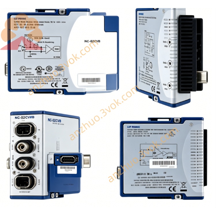
NI PXIe-7975R FlexRIO Reconfigurable PXIe FPGA Module
Description
Product Introduction
The NI PXIe-7975R is a 3U single-slot PXIe FlexRIO high-performance programmable FPGA module, based on Kintex-7 architecture. It offers a comprehensive upgrade in FPGA resources, memory capacity, and bandwidth compared to 7965R/7966R. It is designed for ultra-high complexity real-time signal processing, ultra-large bandwidth data streams, high-density I/O, and multi-module collaboration scenarios. It is suitable for 5G/6G baseband, radar, high-end semiconductor testing, medical imaging, high-speed parallel acquisition, and AI inference acceleration, etc.
Model Interpretation
PXIe: PXI Express Gen2 x4 bus, 3U single slot, compatible with x4/x8/x16 mixed slots.
7975: FlexRIO Kintex-7 series, 75 represents the flagship model of XC7K410T and 2GB DDR3.
R: Reconfigurable I/O, allowing users to customize FPGA logic, I/O, and timing, and perform hardware reprogramming. Technical Specifications
FPGA Core
Chip: Xilinx Kintex-7 XC7K410T, 63,550 logic units, 1,540 DSP48 slices, 28,620 Kb block RAM, with DSP resources being 2.4 times that of 7966R.
Development: Supports LabVIEW FPGA, C/C++, Python, complex filtering hardwareization, FFT, MIMO, beamforming, protocol parsing, AI operators, etc.
On-board Memory
Capacity: 2 GB DDR3 (Single Bank).
Bandwidth: Peak 10.5 GB/s, 3.3 times that of 7966R, supporting large cache and burst throughput.
Bus and Throughput
PXIe: x4 Gen2, bidirectional 3.2 GB/s, unidirectional 1.6 GB/s, bandwidth doubled.
DMA: 32 independent channels, maximum 1.6 GB/s per module.
P2P: Supports multi-module point-to-point transmission, 1.6 GB/s rate, microsecond-level latency, no host intermediate transfer.
Clock: PXI_CLK10, 100 MHz PXIe_Sync100, multi-region clock input, picosecond-level synchronization.
Digital I/O
Channels: 136 single-ended, can be configured with 68 differential pairs (4 more than 7966R).
Rate: Single-ended 400 Mb/s, LVDS differential 1 Gb/s.
Level: 1.2 V/1.5 V/1.8 V/2.5 V/3.3 V, LVDS/LVTTL.
Trigger: Star trigger, D-Star LVDS trigger, PXIe_Sync100, multi-device synchronization.
Physics and Environment
Size: 3U standard (16.1 cm × 10.8 cm, without connectors).
Weight: Approximately 240 g.
Power Consumption: +3.3 V 4 A, +12 V 3 A (including adapter).
Operating Temperature: 0–55 ℃, industrial-grade stable operation.
Interfaces and Communications
Host Bus
PXIe x4 Gen2, connects backplane clock, star trigger, D-Star trigger, Sync100, high-speed synchronization and data routing within the chassis.
Front Panel
High-density edge connectors, dedicated FlexRIO adapter interface, connects to NI 5791/5781/5734 and other RF / analog / digital adapters, expands RF transceivers, high-speed analog I/O, no independent signal ports on the module body.
Drivers and Software
Drivers: NI-FlexRIO, NI-DAQmx, IVI standard, NI-MAX configuration self-check.
Programming: LabVIEW FPGA, C/C++, Python, full API for FPGA development, I/O configuration, P2P routing, trigger control.
Core Functions
Flagship-level FPGA acceleration: Kintex-7 410T, massive DSP and logic resources, supports hardwareization of ultra-complex algorithms, low latency high throughput.
Ultra-large capacity cache: 2 GB DDR3, 10.5 GB/s bandwidth, shares bus pressure, suitable for long-time sequence acquisition, ultra-large batch processing and AI cache.
High-density high-speed configurable I/O: 136 multi-level / differential, parallel testing, high-speed digital interaction and multi-channel synchronous acquisition.
High-bandwidth low-latency P2P transmission: 1.6 GB/s direct inter-module communication, microsecond-level latency, multi-module collaborative system. Precise Synchronization: PXI clock / trigger / Sync100, picosecond-level timing alignment for multiple devices.
Flexible Expansion: Combined with FlexRIO adapter, expand RF transceiver, high-speed analog acquisition, and dedicated digital interfaces. Applicable scenarios
Radio Frequency and Wireless Communication: 5G/6G baseband real-time processing, Massive MIMO, radar signal processing, beamforming, satellite communication prototype.
Semiconductor Testing: High-speed digital testing, SoC / chip protocol analysis, large-scale parallel testing, timing verification, AI chip testing.
Medical Imaging: MRI/CT receiver, real-time DDC and 3D signal processing, high-speed image reconstruction.
High-speed Image Acquisition: 4K/8K front-end real-time preprocessing, AI inference, multi-camera synchronous acquisition.
Industrial Control: Hardware real-time bus, high-precision motion control, industrial robot real-time algorithms, high-speed data recording.
Research Prototypes: Ultra-large-scale algorithm verification, communication architecture hardware implementation, AI edge computing prototype, high-speed physical experiment data processing.
Usage and Maintenance Use
Disconnect the power supply, insert the 3U PXIe chassis, tighten the screws, and strictly prohibit hot swapping. Take measures to prevent static electricity. The adapter also needs to be disconnected for connection and locked. NI-MAX identifies the configuration of I/O levels, clocks, and triggers, downloads the FPGA program for execution. Multiple modules synchronize with a unified reference clock (priority Sync100), configure P2P routing and triggers, and verify the synchronization accuracy. Maintenance
Regularly wipe the module and connectors with a dry cloth, remove dust to maintain good contact, and strictly avoid contact with liquids. Update the driver and firmware of NI-MAX regularly. Store it for a long time in a dry environment at -20 to 60 ℃ with humidity less than 60%, and seal it in an anti-static package. For abnormalities, first check the power supply, adapter connection, and software configuration; for transmission/logic abnormalities, troubleshoot the FPGA program, channel parameters, and P2P routing.
Get a Quote