
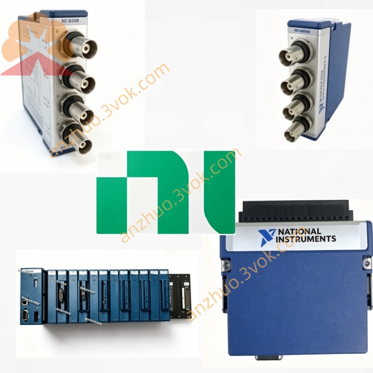
NI PXIe-7965R FlexRIO Reconfigurable PXIe FPGA Module
Description
Product Introduction
The NI PXIe-7965R is a 3U single-slot PXIe FlexRIO user-programmable FPGA module, designed for high-performance real-time signal processing and custom hardware acceleration. It is equipped with Xilinx Virtex-5 SX95T FPGA and integrates 512 MB (2×256 MB) onboard DDR2 DRAM. Compared to 7962R, it offers more FPGA resources and the same cache capacity, making it suitable for more complex algorithms and large data flow scenarios. It is widely used in radio frequency communication, semiconductor testing, high-speed image acquisition, industrial control, and research prototype development.
Model Interpretation
PXIe: PXI Express bus, 3U single slot, compatible with x4/x8/x16 PXIe mixed slots, Gen1 bus, plug-and-play.
7965: NI FlexRIO FPGA series, 65 represents Virtex-5 SX95T and 512 MB DDR2 high-end model.
R: RIO (Reconfigurable I/O), allowing users to customize FPGA logic, I/O, and timing, and reprogram the hardware. Technical Specifications
FPGA Core
Chip: Xilinx Virtex-5 SX95T, 58,880 LUTs/triggers, 640 DSP48 slices, 8784 Kb block RAM.
Development: Supports LabVIEW FPGA, C/C++, Python, and can implement hardware-based filtering, FFT, modulation and demodulation, protocol parsing, etc.
Onboard Memory
Capacity: 512 MB DDR2 (2×256 MB independent banks).
Bandwidth: Peak 3.2 GB/s, supports local cache, frame storage and burst data processing.
Bus and Throughput
PXIe: x4 Gen1, bidirectional 1.4 GB/s, unidirectional > 700 MB/s.
DMA: 16 independent channels, single module up to 800 MB/s.
P2P: Supports multi-module point-to-point transmission, latency in microsecond level, no host intermediate.
Digital I/O
Channels: 132 single-ended, can be configured with 66 differential pairs.
Rates: Single-ended 400 Mb/s, LVDS differential 1 Gb/s.
Levels: 1.2 V/1.5 V/1.8 V/2.5 V/3.3 V, LVDS/LVTTL.
Clocks/Triggers: PXI_CLK10, star trigger, D-Star LVDS trigger, multi-region clock input.
Physics and Environment
Size: 16.1 cm × 10.8 cm (without connectors).
Weight: Approximately 220 g.
Power Consumption: +3.3 V 3 A, +12 V 2.2 A (including adapter).
Operating Temperature: 0–55 ℃, industrial-grade stable operation.
Host Bus
PXIe x4 Gen1, connects backplane clock, star trigger, D-Star trigger, realizes synchronization and data routing within the chassis for NI.
Front Panel
High-density card edge connector, dedicated FlexRIO adapter interface, connects NI 5791/5781 and other RF/digital adapters, expands analog/RF I/O, no independent signal ports for the module itself for NI.
Drivers and Software
Drivers: NI-FlexRIO, NI-DAQmx, IVI standard, NI-MAX configuration self-check.
Programming: LabVIEW FPGA, C/C++, Python, complete API for FPGA development, I/O configuration, P2P routing and trigger control.
Core Functions
High-performance FPGA acceleration: Virtex-5 SX95T has abundant resources, can deploy complex algorithms, hardware acceleration reduces CPU load.
Large-capacity local cache: 512 MB DDR2 shares bus pressure, suitable for long-time sequence acquisition and batch processing.
High-speed configurable I/O: 132 channels, multi-level/differential, meets parallel testing, high-speed digital interaction.
Low-latency P2P transmission: Direct data exchange between modules, microsecond-level latency, suitable for multi-channel synchronous systems.
Precise synchronization: PXI clock/trigger resources, multi-device picosecond-level timing alignment for NI.
Flexible Expansion: Combined with FlexRIO adapter, expands RF transceiver, analog acquisition, dedicated digital interface for NI. Applicable scenarios
Radio Frequency and Wireless Communication: Radar, 5G/6G Baseband Real-time Processing, Modulation and Demodulation, Beamforming NI.
Semiconductor Testing: High-speed Digital Testing, Protocol Parsing, Parallel Testing, Timing Verification NI.
High-speed Image Acquisition: Front-end Real-time Preprocessing, Reducing Back-end Transmission and Computing Pressure NI.
Industrial Control: Hardware to Implement Real-time Bus Protocols, High-precision Motion Control, Improving Response Speed NI.
Research Prototypes: Algorithm Verification, Signal Processing and Hardware Implementation of Communication Architecture, Rapid Iteration NI.
Usage and Maintenance Use
Disconnect the power supply, insert the 3U PXIe chassis, tighten the screws, and strictly prohibit hot swapping. Take precautions against static electricity. Connect the adapter under the same power-off condition, align and lock it. NI-MAX identifies the configuration of I/O levels, clocks, and triggers, downloads the FPGA program for operation. Multiple modules synchronize with a unified reference clock, configure P2P routing and triggers, and verify the synchronization accuracy. Maintenance
Regularly wipe the module and connectors with a dry soft cloth, remove dust, and ensure good contact. Do not allow contact with liquids. Update the driver and firmware of NI-MAX regularly. Store it for a long time in a dry environment at -20 to 60 ℃ with humidity less than 60%, and seal it in an anti-static package. When there is an anomaly, check the power supply, adapter connection, and software configuration; for transmission errors or logical anomalies, troubleshoot the FPGA program, channel parameters, and P2P routing.
Get a Quote