
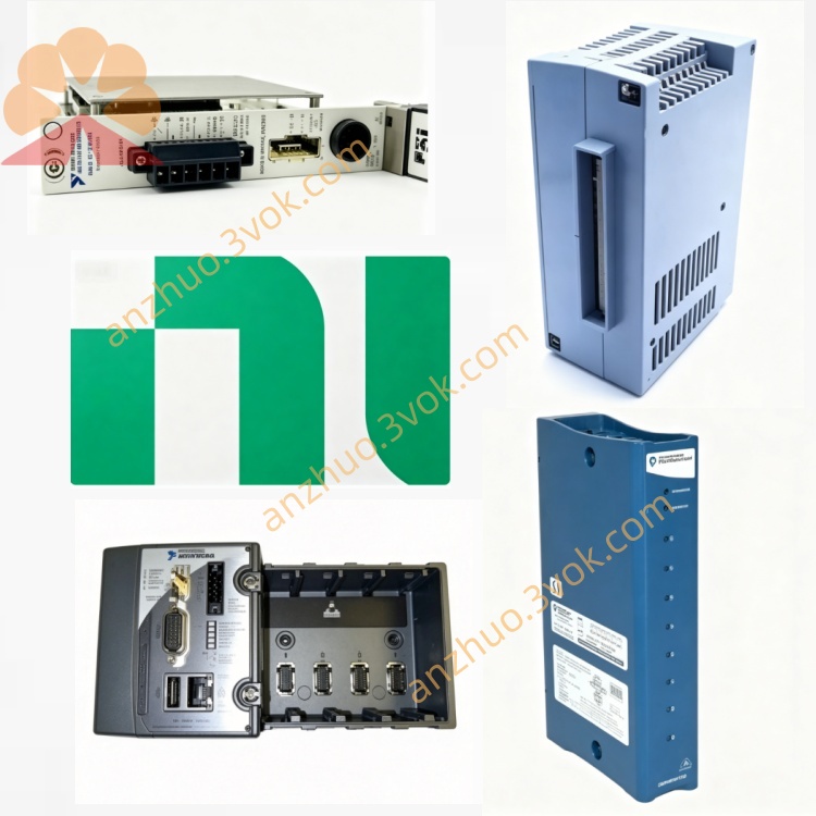
NI PXIe-7962R Mid-range FlexRIO Reconfigurable PXIe FPGA Module
Description
Product Introduction
The NI PXIe-7962R is a 3U single-slot PXIe FlexRIO reconfigurable I/O module, equipped with an Xilinx Virtex-5 SX50T programmable logic chip and a built-in 512 MB DDR2 large-capacity memory. The module expands external signal interfaces through an external adapter and has local high-speed data cache, hardware-level real-time computing, and low-latency data interaction capabilities. It is suitable for large data flow processing, high-speed signal algorithm acceleration, and the implementation of custom communication protocols, and is widely used in radio frequency communication, semiconductor testing, and image acquisition fields.
Model Interpretation
PXIe represents that the module adopts the PXI Express bus and follows the 3U single-slot mechanical standard, which is compatible with the conventional PXIe chassis slots. 7962 belongs to the NI FlexRIO programmable FPGA series model. This model is equipped with the Virtex-5 SX50T chip and integrates onboard DDR2 memory. The suffix R represents reconfigurable I/O. Users can independently write, burn, and program FPGA logic codes, flexibly define hardware functions, interface modes, and timing rules. Technical Specifications
FPGA core resources
The module is equipped with the Xilinx Virtex-5 SX50T chip, featuring 8,160 logic slices, 2,888 DSP computing units, and 4,752 kilobit block memory. It supports both graphical and code-based development methods, enabling the deployment of signal processing algorithms, custom bus protocols, and precise timing control logic on the hardware side.
Onboard memory
It is equipped with 512 MB DDR2 dynamic memory, with a peak memory access bandwidth of up to 3.2 GB/s, capable of performing local caching of high-speed data streams, data frame storage, and temporary processing of burst data, effectively reducing the burden on the bus transmission.
Bus and transmission performance
It adopts the PXIe Gen1 x4 bus, with a bidirectional peak bandwidth of 1.4 GB/s, and a single-direction transmission bandwidth exceeding 700 MB/s. It is equipped with sixteen independent DMA channels, with a maximum data stream rate of 800 MB/s per module. It natively supports point-to-point transmission between modules, eliminating the need for data interaction to pass through the upper host, significantly reducing transmission latency.
Digital I/O electrical parameters
The module provides 132 digital channels, which can be configured as single-ended mode or used in a 66-channel differential channel combination. The maximum transmission rate of single-ended signals is 400 Mb/s, and the LVDS differential signal rate can reach 1 Gb/s. It is compatible with multiple logic levels of 1.2 V, 1.5 V, 1.8 V, 2.5 V, and 3.3 V, and supports both LVDS and LVTTL electrical standards. It can be connected to the PXI backplane clock, star trigger, and D-Star LVDS trigger signals, meeting the requirements for multi-module high-precision synchronization.
Physical and environmental parameters
The module is a 3U standard size, weighing approximately 220 grams. When used with an adapter, the 3.3 V supply current is 3 amperes, and the 12 V supply current is 2.2 amperes. The standard operating temperature range is 0 degrees Celsius to 55 degrees Celsius, allowing for long-term stable operation in industrial test environments.
Interface and communication configuration
Host bus interface
The module uses the PXIe Gen1 x4 bus, supporting plug-and-play, and can fully utilize the clock, star trigger, D-Star high-speed trigger and other synchronization resources on the chassis backplane to achieve timing alignment and data routing management of multiple modules within the chassis.
Front panel interface
The panel is equipped with high-density edge connectors as dedicated expansion interfaces, used to connect various FlexRIO adapter modules, thereby expanding external signal interfaces such as RF, analog, and high-speed digital, with the module body having no independent external signal ports.
Driver and software communication
The accompanying driver is NI-FlexRIO and NI-DAQmx, compliant with the IVI universal instrument specification. Through NI-MAX, it can complete hardware identification, device self-check, basic parameter configuration, and firmware version management. It supports mainstream development environments such as LabVIEW FPGA, C/C++, and Python, providing a complete set of application programming interfaces, enabling FPGA logic development, channel parameter setting, point-to-point transmission routing, and trigger strategy configuration. The point-to-point transmission function between modules enables low-latency data communication and is suitable for large-scale multi-channel synchronous processing systems. Relying on the abundant clock and trigger resources of the PXI backplane, a multi-module and multi-device synchronous system can be built. By combining with different specifications of FlexRIO adapters, functions such as RF transmission and reception, analog acquisition, and dedicated digital interfaces can be flexibly expanded to meet diverse testing requirements. Applicable scenarios
In the field of radio frequency and wireless communication, it can be applied to the real-time processing, modulation and demodulation, and beamforming development of baseband signals for radar and mobile communication systems. In semiconductor and chip testing, it is used to build a custom high-speed digital test platform to achieve chip protocol parsing, parallel testing and timing verification. In high-speed image and data acquisition scenarios, it can perform real-time pre-processing of images and sensor data at the front end, reducing the pressure on subsequent transmission and computation. In the field of industrial control, it can be used to implement industrial real-time bus protocols and high-precision motion control logic, improving the system response speed. It is also applicable to various research projects and algorithm prototype verification, quickly completing the hardware implementation and scheme iteration of signal processing and communication architecture.
User and Maintenance Instructions Instruction Manual
When the power is off, insert the module into the standard 3U PXIe chassis slot and tighten the fixing screws. During the operation of the equipment, hot plugging is strictly prohibited. During the operation, take precautions against static electricity. When connecting the adapter, also perform the operation with the power off to ensure that the interface is aligned and locked, and avoid damaging the interface pins. After powering on, complete the hardware identification through NI-MAX, configure the I/O levels, clock sources and trigger modes as needed, and then download the compiled FPGA program to the chip for operation. When building a multi-module synchronous system, unify the reference clock of all devices, configure point-to-point transmission routes and trigger signals, and verify the synchronization accuracy before conducting the test work.
Maintenance Instructions
Regularly use a dry soft cloth to wipe the module surface and connectors, clean the surface dust, keep the interface in good contact, and strictly prohibit contact with liquids to prevent corrosion and short-circuit faults. Regularly check and update the drivers and firmware through NI-MAX to ensure the stability of the equipment operation. When the module is idle for a long time, place it in a dry environment ranging from -20°C to 60°C with a relative humidity of less than 60%, and seal it in an anti-static packaging. When the equipment has abnormalities, prioritize checking the power supply status, adapter connection, and software configuration; if there are data transmission errors or logical operation abnormalities, sequentially check the FPGA program, channel parameters and transmission route settings.
Get a Quote