
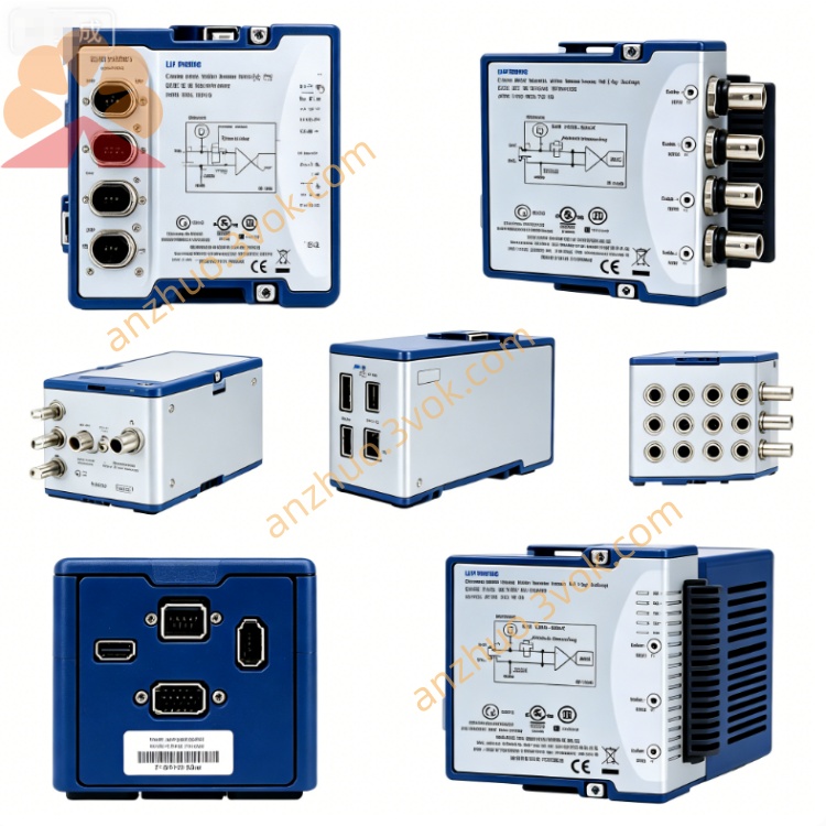
NI PXIe-6674T OCXO High Precision Timing & Synchronization Module
Description
Product Introduction
The NI PXIe-6674T is a 3U single-slot PXIe high-performance timing synchronization master module launched by National Instruments (NI). It is equipped with an oven-controlled crystal oscillator (OCXO) and a high-speed DDS circuit as its core, providing an ultra-high stability reference clock and picosecond-level synchronization capability for the PXIe system. It can directly replace the default PXI_CLK10 backplane clock of the chassis and fully supports PXI star-triggering and D-Star high-speed LVDS triggering. It is suitable for multi-chassis distributed testing, radio frequency communication, semiconductor testing, aerospace and other scenarios with strict requirements for timing accuracy and stability. It is the top-level timing synchronization unit of the PXI platform by NI.
Model Interpretation
PXIe: PXI Express bus architecture, 3U single-slot specification, compatible with Gen1 x1 bus, supports plug-and-play and full coverage of backplane resources by NI.
6674: NI's high-end timing synchronization series number, representing the flagship model equipped with OCXO oven-controlled crystal oscillator, supporting 1GHz DDS and LVDS triggering by NI.
T: Timing, the core of system-level timing distribution and trigger routing, without counting / general digital IO functions, focusing on timing synchronization by NI. Technical Specifications
Board-mounted clock core parameters
OCXO reference: 10 MHz, accuracy within ±80 ppb after calibration within one year, stability in the full temperature range (0–55℃) is much better than that of TCXO, with extremely small annual drift NI.
DDS output: frequency range DC–1 GHz, resolution 0.075 Hz, reference PXIe_CLK100 (800 MHz phase-locked), supports wideband programmable clock output NI.
Synchronization accuracy: system synchronization jitter < 100 ps, offset between trigger channels (skew) < 50 ps, extremely low phase noise, meeting the requirements for high-precision phase synchronization.
Electrical and environmental parameters
Interface impedance: 50 Ω for all signal ports, AC coupling, compatible with standard RF / clock cables NI.
Clock input: 1 MHz–1 GHz, compatible with sine wave / square wave, supports external high-precision clock source access NI.
Clock output: selectable 1.0 Vpp/2.5 Vpp dual amplitude, compatible with different instrument interface levels NI.
PFI trigger: 6 programmable channels (PFI0–PFI5), single-ended 0–5 V or LVDS differential optional, maximum working frequency 1 GHz NI.
Power consumption / temperature: typical power consumption approximately 15 W; operating temperature 0–55℃, meeting the requirements for long-term stable operation of industrial-grade systems.
Interface and communication configuration
Host bus interface
PXIe Gen1 x1 bus, can cover and replace the default PXI_CLK10 backplane clock of the chassis, fully connect PXI star trigger, D-Star A/B/C three-channel LVDS high-speed trigger resources, realize flexible routing and synchronous control of signals within the chassis NI.
Front panel interface (8 SMA ports)
CLKIN: external clock input (SMA), connects external 1 MHz–1 GHz reference source NI.
CLKOUT: clock output (SMA), outputs OCXO reference or DDS clock to other chassis/instruments NI.
PFI0–PFI5: 6 programmable triggers (SMA), single-ended / LVDS optional, configured as input or output, transmits trigger / event signals NI.
Driver and software communication
Standard NI-DAQmx driver, compliant with IVI standard, compatible with NI-MAX software for hardware identification, parameter configuration and self-check NI.
Supports mainstream development environments such as LabVIEW, C/C++, Python, TestStand, etc., provides complete API for clock setting, trigger routing configuration and synchronization strategy editing NI.
Core functions
Provides ultra-highly stable 10 MHz OCXO reference clock, replacing the default clock of the chassis, significantly improving the accuracy and long-term stability of the system timing reference NI.
Outputs wideband programmable clock from DC–1 GHz DDS, meeting the clock requirements of multiple devices for high-speed acquisition, RF testing, digital testing, etc. NI.
Supports clock and trigger cascading between multiple PXIe chassis, builds a distributed test system with a unified time domain, with synchronization accuracy reaching picosecond level.
Can connect external high-precision reference sources such as GPS slave clock, rubidium atomic clock, and can output a standard clock, achieving phase synchronization with third-party instruments NI.
Flexible routing of PXI star trigger and D-Star LVDS trigger signals, links various modules within the chassis, ensures precise and orderly execution of the test process NI. Applicable scenarios
Radio Frequency and Wireless Communication Testing: 5G/6G, radar, MIMO systems, ensuring strict consistency in phase and timing of multi-channel radio frequency equipment.
Semiconductor and Integrated Circuit Testing: Parallel testing of high-speed digital chips and radio frequency chips, achieving synchronous control at multiple stations and precise timing alignment.
Aerospace and Defense Industry: Satellite navigation, radar signal processing, electronic warfare systems, requiring high-stability clocks and picosecond-level synchronization accuracy NI.
Distributed Multi-Rack Data Acquisition: Vibration, acoustics, modal analysis, etc., achieving precise synchronous acquisition of dozens or hundreds of channels of signals.
High-Precision Measurement and Calibration: As a standard clock source, calibrating the timing accuracy of other testing instruments to ensure the traceability of measurement values NI.
User and Maintenance Instructions Instruction Manual
Installation: Insert the standard 3U PXIe chassis system timing slot, tighten the fixing screws, and prohibit hot swapping; take precautions against static electricity during operation.
Wiring: Use 50 Ω coaxial cables for the clock/trigger signals, keep the control cable lengths consistent to reduce signal attenuation and reflection; correctly connect CLKIN/CLKOUT and PFI interfaces according to the signal flow direction.
Configuration: Select the clock source (board-mounted OCXO / external input), set the DDS frequency, and configure the PFI trigger mode and routing strategy through NI-MAX or programming environment.
Multi-box synchronization: Set the reference clock for all boxes uniformly, cascade the D-Star trigger bus, verify the synchronization accuracy, and ensure the consistency of multi-box timing.
Maintenance instructions
Daily cleaning: Regularly wipe the panel and interfaces with a dry soft cloth, remove dust, and keep the contact good; do not allow liquid contact with the modules, to avoid corrosion and short circuits.
Calibration cycle: It is recommended to conduct professional calibration once every 1-2 years to ensure that the OCXO accuracy, DDS frequency accuracy, and trigger synchronization accuracy meet the standards.
Storage: When in a long-term idle state, store it in a dry environment of -20 to 60℃ with a relative humidity of less than 60%, use anti-static packaging, and avoid high temperature, humidity, and static damage.
Fault troubleshooting: When there is an anomaly, prioritize checking the cable connections, power supply status, and software configuration; if there is frequency deviation, synchronization failure, focus on checking the clock source, transmission lines, and DDS parameter settings.
Get a Quote