
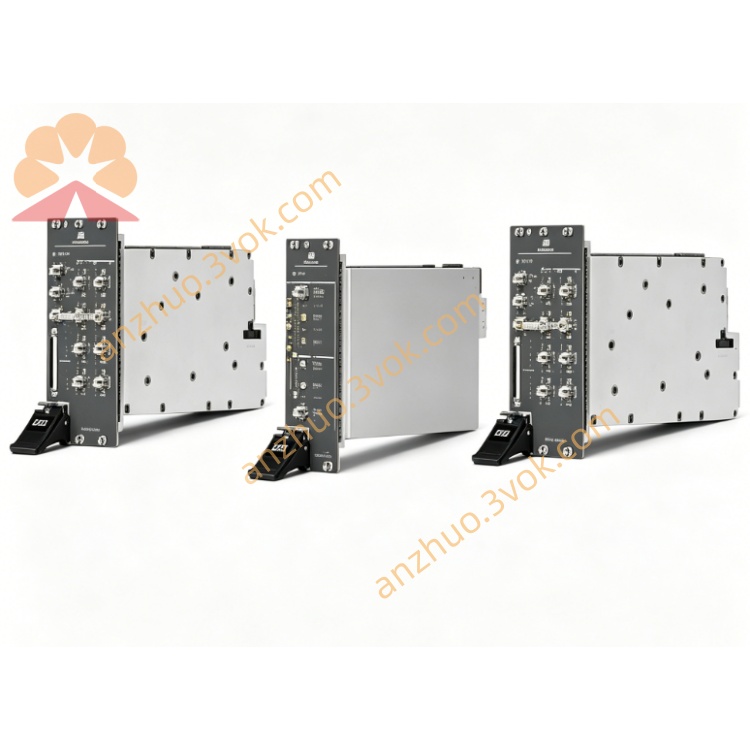
NI PXIe-6672 TCXO Timing Synchronization Module
Description
Product Introduction
The PXIe-6672 is a 3U single-slot PXIe system timing synchronization module launched by NI. It is equipped with a temperature-compensated crystal oscillator and a direct digital frequency synthesis circuit, serving as the clock and synchronization core of the entire PXI test system. This module can output high-stability reference clocks and programmable frequency clocks, and also has a complete trigger signal routing capability. It can achieve high-precision timing alignment between single-box multiple modules, multiple-boxes, and external instruments, with synchronization accuracy reaching picosecond level. It is mainly targeted at various test and measurement systems with strict requirements for clock stability and timing synchronization.
Model Interpretation
PXIe represents the PXI Express bus architecture, adopting the industry-standard 3U single-slot hardware specification. 6672 is the dedicated timing synchronization module number of NI, representing the system synchronization unit integrating a temperature-compensated crystal oscillator reference and a wide-band DDS clock. This module is positioned as a system-level clock distribution and trigger management device, without counting, general digital input/output functions. Its core features include onboard reference clock, wide-range programmable clock, and multiple programmable trigger channels, fully compatible with various synchronization resources on the PXI backplane. Technical Specifications
Board-mounted clock parameters
The module is equipped with a 10 MHz temperature-compensated crystal oscillator as the reference clock. Within the temperature range of 0°C to 55°C, the initial frequency accuracy is ±3.5 ppm, and the annual frequency drift is approximately ±1 ppm, ensuring long-term stable operation. An integrated DDS circuit is also included, with the output clock frequency range covering from DC to 105 MHz, and the frequency adjustment resolution reaching 0.075 Hz. The overall synchronization accuracy can reach 100 picoseconds, and the offset between trigger signals is less than 50 picoseconds.
Electrical and environmental parameters
The impedance of all signal ports on the front panel is 50 ohms. The external clock input supports signals ranging from 1 MHz to 105 MHz, compatible with both sine wave and square wave waveforms. The clock output provides two amplitude levels: 1.0 V peak-to-peak and 2.5 V peak-to-peak. Six programmable trigger channels are equipped, with an input voltage range of 0 V to 5 V and a maximum working frequency of 105 MHz. The module typically consumes about 12 W of power, and the standard operating temperature range is 0°C to 55°C.
Interface and communication configuration
Host bus interface
The module adopts the PXIe Gen1 x1 bus, supporting plug-and-play functionality. It can replace the default PXI_CLK10 backplane clock of the chassis, and fully utilize the backplane resources such as PXI star trigger and D-Star high-speed trigger to achieve flexible routing and synchronous control of various signals within the chassis.
Front panel interface
One external clock input interface is provided for connecting external high-precision clock source signals. One clock output interface is available to output the onboard clock signal to other chassis or external instruments. Six independent programmable trigger ports are provided, which can be configured as input or output modes as needed, for transmitting trigger signals and interactive events.
Driver and software communication
The standard NI-DAQmx driver program complies with the IVI industry standard. Users can complete hardware identification, parameter configuration, and device self-check and debugging through the NI-MAX software. It supports mainstream development environments such as LabVIEW, C/C++, Python, and TestStand, and provides complete application programming interfaces for clock parameter setting, trigger routing configuration, and synchronization strategy editing.
Core functions
It can provide a highly stable 10 MHz base clock for the entire PXI chassis, enhancing the timing reference performance of the entire system. The wideband DDS clock output can meet the clock requirements of various devices such as high-speed data acquisition, digital testing, and RF testing. It supports cascading clock and trigger signals between multiple PXI chassis, allowing the distributed test system to be in a unified time domain. It can be connected to external high-precision reference sources such as GPS clocks and rubidium atomic clocks, and can also output a standard clock to achieve synchronization with third-party test instruments. Relying on the flexible trigger routing function, it can link different functional modules within the chassis to ensure the orderly execution of the test process. Applicable scenarios
Suitable for distributed multi-box data acquisition scenarios in vibration, acoustics, dynamic signals, etc., it enables precise timing alignment of multiple signals. In RF and wireless communication tests, it ensures that the phases and timings of multiple RF devices remain consistent. It is used in semiconductor and integrated circuit testing fields to complete synchronous control of multi-station parallel testing systems. Widely applied in aerospace, national defense, and precision measurement fields, it meets the requirements of high timing stability and synchronization accuracy. It can also be deployed in large-scale automated production lines to provide a unified clock and trigger signal for the entire set of production testing equipment.
User and Maintenance Instructions Instruction Manual
Install the module into an empty slot of the standard 3U PXIe chassis and tighten the fixing screws. Use the matching 50-ohm coaxial cable for the clock and trigger signal lines. Reasonably control the cable length to avoid signal attenuation and reflection problems. Complete the related configurations such as clock source selection, frequency parameters, and trigger routing through the matching software. When building a multi-box synchronization system, uniformly set the reference clock for the entire set of equipment in advance and check the connection status of the cascaded lines. During equipment operation, prohibit hot plugging and take anti-static protection measures when operating.
Maintenance Instructions
Regularly wipe the equipment panel and interfaces with a dry soft cloth to remove surface dust and keep the contact good. Do not allow liquid contact with the module body. It is recommended to conduct professional calibration of the clock accuracy and trigger performance once every two years. When the equipment is idle for a long time, store it in a dry environment with a temperature of -20°C to 60°C and a relative humidity of less than 60%, and use anti-static packaging for protection. When the equipment has abnormalities, prioritize checking the line connection, power supply status, and software configuration; if there are frequency deviations or synchronization failure issues, focus on troubleshooting the clock source and transmission lines.
Get a Quote