
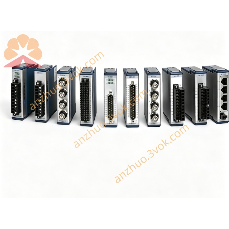
NI PXIe-5450 145MHz Dual Channel I/Q Arbitrary Waveform Generator
Description
Model Nomenclature
PXIe: PXI Express high‑speed modular instrumentation bus.
54: NI PXI waveform generator series.
50: High‑speed 16‑bit dual‑channel I/Q AWG, 400 MS/s, 145 MHz bandwidth, differential outputs, deep memory, and advanced OSP for communications/radar I/Q signals.
Technical Specifications
Form Factor: 3U single‑slot PXIe module.
Channels: 2 fully independent differential analog output channels (I/Q pair).
Bandwidth: 145 MHz (‑3 dB, 50 Ω single‑ended); 120 MHz I/Q bandwidth.
Sampling Rate: 400 MS/s (max, interpolated); 100 MS/s (native).
Resolution: 16‑bit vertical resolution.
Output Impedance: 50 Ω (single‑ended); 100 Ω (differential, nominal).
Voltage Range: 1 Vpp differential (into 100 Ω); ±0.5 V (single‑ended).
Onboard Memory: 128 MB (780419‑01) or 512 MB (780419‑02), shared for waveforms/instructions.
SFDR: >98 dB (close‑in, 1 MHz, no harmonics, typical).
Phase Noise: <‑140 dBc/Hz @10 MHz (1 kHz offset, typical).
Skew: <25 ps channel‑to‑channel (typical).
Waveform Types: Standard (sine, square, triangle, ramp); arbitrary (user‑defined I/Q sequences).
Onboard Processing: FIR/interpolation filters, pulse shaping, digital gain/offset, NCO, IQ mixing, flatness correction.
Environmental: Operating 0 °C to 55 °C; Storage ‑40 °C to 70 °C.
Connectors: Front‑panel SMA (differential outputs), SMB (CLK IN/OUT, trigger), PFI lines.
Interface and Communication Configuration
Bus: PXIe Gen1 x1, high‑speed DMA streaming.
Drivers: NI‑FGEN, NI‑DAQmx, IVI‑COM for Windows.
Software Support: NI‑MAX (config/diagnostics); LabVIEW, C/C++, Python, .NET for automation.
Synchronization: PXI trigger bus, star trigger, NI‑TClk (picosecond‑level alignment with PXIe digitizers/instruments).
Clock: Internal high‑resolution VCXO (±25 ppm); external 10 MHz reference IN/OUT; external sample clock (10 S/s to 105 MS/s).
Data Transfer: DMA for continuous streaming; peer‑to‑peer sharing with other PXIe modules.
Core Features
Dual‑Channel 16‑Bit I/Q Output: Differential design delivers high fidelity for baseband/IQ signals, ideal for direct I/Q device testing.
400 MS/s & 145 MHz Bandwidth: Wide bandwidth and high sampling support 5G/6G, radar, and satellite communications signals.
FPGA‑Based OSP: Reduces host load, accelerates waveform download, enables real‑time filtering, gain control, and frequency shifting via NCO.
Deep Memory: Up to 512 MB supports long‑record waveforms and multi‑sequence playback without host intervention.
Ultra‑Low Skew & High Spectral Purity: <25 ps skew ensures phase coherence; >98 dB SFDR minimizes distortion for sensitive RF/communications test.
Flexible Synchronization: NI‑TClk and PXI star trigger enable phase‑coherent multi‑channel operation for MIMO and beamforming systems.
Application Scenarios
Wireless Communications: 5G/6G baseband I/Q generation, wideband IF test, transceiver prototype validation, and MIMO system test.
Aerospace & Defense: Radar pulse/Chirp I/Q simulation, electronic warfare (EW) waveform generation, satellite communication transceiver test.
RF Vector Signal Generation: Baseband I/Q core for PXIe‑5673E and other NI RF VSG systems.
Semiconductor Test: High‑speed mixed‑signal validation, I/Q interface characterization, and precision clock/power transient simulation.
Research & Development: Physics experiment signal generation, ultrasonic testing, and general‑purpose high‑fidelity arbitrary waveform applications.
Get a Quote