
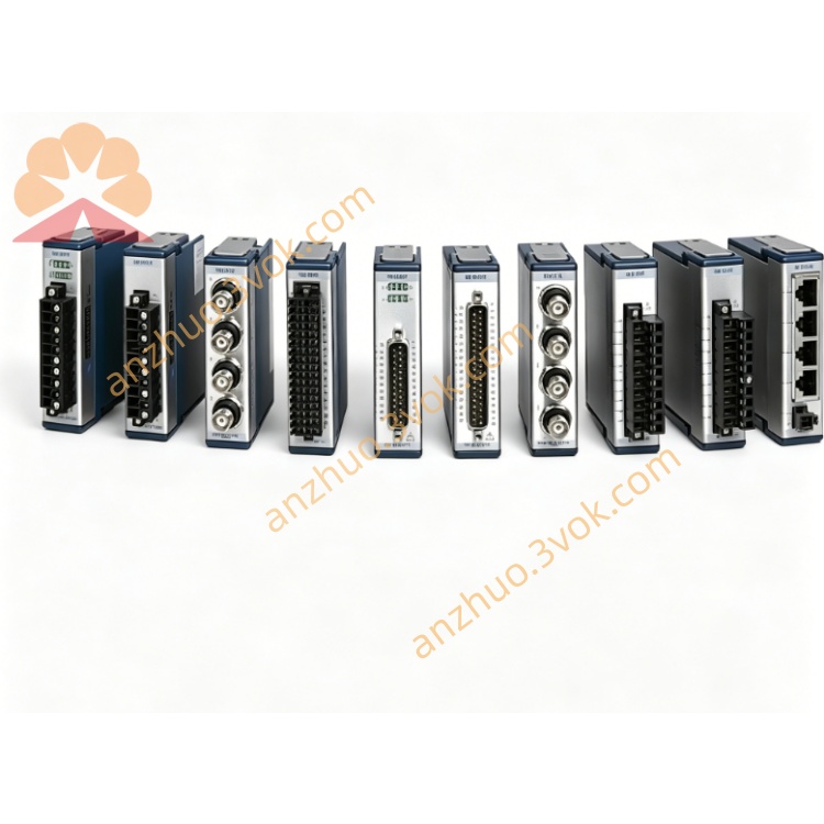
NI PXI-6653 Timing Synchronization PXI Module
Description
II. Model Interpretation
PXI: Standard 3U single slot, compatible with PXI/PXIe mixed slots, dedicated Slot 2 star trigger controller position, connects backplane clock, trigger, and star trigger bus.
6653: 665x Precision Timing Series, 3 represents the OCXO ultra-high-precision master clock model, with built-in constant temperature crystal oscillator, master-slave integrated, the highest specification of the series.
Position: Ultra-high stability system master clock, targeted for RF, aerospace, semiconductor, etc. demanding timing scenarios.
III. Technical Parameters (25℃)
1. Clock and Frequency
Built-in reference: OCXO 10 MHz, stability 50 ppb (±3.2 ppb typical)
DDS output: DC ~ 105 MHz, resolution 711 nHz
External clock input: 1 MHz ~ 105 MHz, sine / square wave compatible
Input / Output impedance: 50 Ω
Synchronization accuracy: multi-box **<1 ns**, backplane trigger skew **<500 ps**
2. Trigger and Synchronization
Programmable PFI: 6 channels (SMB), input / output configurable
Backplane bus: control 8 channels PXI_TRIG, 13 channels PXI_STAR star trigger
Clock routing: replace / forward PXI_CLK10, support external reference phase-locked loop (PLL)
Trigger skew: PXI_STAR 400 ps, PFI 500 ps
3. Physical and Environmental
Form: 3U single slot
Connectors: front panel 8×SMB (CLKIN, CLKOUT, PFI0~PFI5)
Status indication: 2 groups of three-color LEDs (Access/Active)
Operating temperature: 0 ℃ ~ 55 ℃
Preheating time: 30 minutes (OCXO stable)
Power consumption: +5 V/2 A, +3.3 V/600 mA, +12 V/500 mA
IV. Interface and Communication Configuration
1. Hardware Interface
Front panel: CLKIN (SMB), CLKOUT (SMB), PFI0~PFI5 (SMB), 50 Ω impedance
Backplane: dedicated Slot 2, linked with 10 MHz reference, 8 channels trigger, 13 channels star trigger bus
2. Software and Drivers
Driver: NI-SYNC, responsible for clock configuration, routing, PLL phase-locked loop, synchronization management
Development environment: supports LabVIEW, C/C++, Python, TestStand, LabVIEW FPGA
Functions: supports custom synchronization logic, phase calibration, frequency measurement
V. Core Functions
OCXO ultra-high stable 10 MHz master clock
Built-in 50 ppb constant temperature crystal oscillator, output ultra-low phase noise 10 MHz reference, replace chassis backplane clock, provide nanosecond-level timing reference for the system.
Ultra-high resolution DDS clock generation
Output DC~105 MHz programmable clock, 711 nHz resolution, suitable for RF modulation, high-speed sampling, precise timing calibration scenarios.
Flexible routing of all channels signals
6 channels PFI, CLKIN/CLKOUT and backplane trigger / star bus freely mapped, supports multi-box cascading, star topology, external device synchronization, builds complex synchronization network.
Seamless switching and locking between master and slave
Independent as the master clock, or receive 10 MHz/GPS reference as the slave, PLL locking accuracy < 1 ns, suitable for single/multi-box expansion.
Low skew multi-device synchronization Special star trigger controller, multi-board / multi-rack synchronization **<1 ns**, trigger skew **<500 ps**, meeting the requirements for high-channel number synchronization acquisition.
VI. Application Scenarios
RF / Microwave Test System
Signal source, spectrum analyzer, vector network analyzer lock the same synchronization to ensure phase consistency and measurement accuracy.
Aerospace / Defense High Precision Measurement and Control
Radar, electronic warfare, satellite testing and other high timing strict scenarios, providing nanosecond-level synchronization reference.
High-channel number data acquisition (≥1000 channels)
Vibration, acoustics, antenna array testing, multi-rack digital instrument / dynamic signal analyzer synchronous acquisition.
Semiconductor chip timing verification
High-speed digital chip, SoC timing test, providing ultra-low skew trigger and clock reference.
Distributed high-precision industrial measurement and control
Multi-site, multi-rack collaboration, time deviation between remote sites controlled within 1 ns.
VII. Usage and Maintenance Instructions
1. Installation and Power On
Disconnect and insert the PXI chassis Slot 2 (forced star trigger position), tighten the screws and ground reliably. After power-on, preheat for 30 minutes to ensure the OCXO stable; keep the chassis ventilated during operation, environmental temperature fluctuation ≤ ±1 ℃, to avoid affecting frequency stability.
2. Wiring and Operation
Interface: Use 50 Ω SMB shielded cable; high-frequency (>10 MHz) signals strictly equal in length, length difference ≤ 1 cm, reducing timing skew.
Mode: Default master mode (output 10 MHz); from mode requires software configuration of PLL lock-in external reference, after locking, LED displays green.
Configuration: Software sets DDS frequency, PFI direction, signal routing, supports FPGA programming to customize synchronization logic.
3. Daily Maintenance
Regularly clean SMB interface, check cable connections, leave a dust cap for long-term idle, to avoid oxidation and dust affecting signal quality.
Calibration: Suggested every 6 months once, use NI Calibration Executive, requires 30 minutes preheating, calibrate OCXO frequency and phase.
Driver Firmware: Regularly update NI-SYNC driver and firmware to ensure compatibility and synchronization stability; discontinued models can be compatible with new firmware versions.
II. Model Interpretation
PXI: Standard 3U single-slot, compatible with PXI/PXIe mixed slots, exclusive Slot 2 position for star trigger controller, connects to the backplane clock, trigger, star trigger bus.
6653: 665x Precision Timing Series, 3 represents the OCXO ultra-high-precision master clock model, built-in constant temperature crystal oscillator, master-slave integrated, the highest specification of the series.
Location: Ultra-high stability system master clock, for strict timing scenarios such as RF, aerospace, semiconductor, etc.
III. Technical Parameters (25℃)
1. Clock and Frequency
Built-in reference: OCXO 10 MHz, stability 50 ppb (±3.2 ppb typical)
DDS output: DC ~ 105 MHz, resolution 711 nHz
External clock input: 1 MHz ~ 105 MHz, sine / square wave compatible
Input / Output impedance: 50 Ω
Synchronization accuracy: multi-rack **<1 ns**, backplane trigger skew **<500 ps**
2. Trigger and Synchronization
Programmable PFI: 6 channels (SMB), input / output configurable
Backplane bus: control 8 channels PXI_TRIG, 13 channels PXI_STAR star trigger Clock Routing: Replace / Forward PXI_CLK10, supports external reference phase-locked loop (PLL)
Trigger Skew: 400 ps between PXI_STAR, 500 ps between PFI
3. Physical and Environment
Form: 3U single slot
Connectors: Front panel 8×SMB (CLKIN, CLKOUT, PFI0~PFI5)
Status Indicators: 2 groups of three-color LEDs (Access/Active)
Operating Temperature: 0 ℃ ~ 55 ℃
Preheating Time: 30 minutes (OCXO stable)
Power Consumption: +5 V/2 A, +3.3 V/600 mA, +12 V/500 mA
IV. Interface and Communication Configuration
1. Hardware Interface
Front panel: CLKIN (SMB), CLKOUT (SMB), PFI0~PFI5 (SMB), 50 Ω impedance
Back panel: Dedicated Slot 2, linked 10 MHz reference, 8 triggers, 13 star-shaped trigger bus
2. Software and Drivers
Driver: NI-SYNC, responsible for clock configuration, routing, PLL locking, synchronization management
Development Environment: Supports LabVIEW, C/C++, Python, TestStand, LabVIEW FPGA
Function: Supports custom synchronization logic, phase calibration, frequency measurement
V. Core Functions
OCXO Ultra-stable 10 MHz Main Clock
Built-in 50 ppb constant temperature crystal oscillator, output ultra-low phase noise 10 MHz reference, replaces the clock on the chassis back panel, provides nanosecond-level timing reference for the system.
Ultra-high resolution DDS clock generation
Output DC~105 MHz programmable clock, 711 nHz resolution, suitable for RF modulation, high-speed sampling, precise timing calibration scenarios.
Flexible routing of all channels of signals
6 PFI, CLKIN/CLKOUT and back panel triggers / star-shaped bus freely mapped, supports multi-chassis cascading, star topology, external device synchronization, builds complex synchronization networks.
Master-slave seamless switching and locking
Can be an independent master clock, or receive an external 10 MHz/GPS reference as a slave, PLL locking accuracy < 1 ns, suitable for single/multi-chassis expansion.
Low skew multi-device synchronization
Special star-shaped trigger controller, multi-board/card / multi-chassis synchronization **<1 ns**, trigger skew **<500 ps**, meets the requirements of high-channel-count synchronization acquisition.
VI. Application Scenarios
Radio frequency / microwave test system
Lock synchronization of signal sources, spectrum analyzers, vector network analyzers to ensure phase consistency and measurement accuracy.
Aerospace / defense high-precision measurement and control
Radar, electronic warfare, satellite testing and other high-time-critical scenarios, provide nanosecond-level synchronization reference.
High-channel-count data acquisition (≥1000 channels)
Digital instruments / dynamic signal analyzers for vibration, acoustics, antenna array testing, multi-chassis digital instruments / dynamic signal analysis synchronization acquisition.
Semiconductor chip timing verification
High-speed digital chips, SoC timing testing, provide ultra-low skew trigger and clock reference.
Distributed high-precision industrial measurement and control
Multi-site, multi-chassis collaboration, time deviation between remote sites controlled within 1 ns.
VII. Usage and Maintenance Instructions
1. Installation and Power On
Disconnect and insert the PXI chassis Slot 2 (forced star-shaped trigger position), tighten the screws and reliably ground. After powering on, preheat for 30 minutes to ensure the OCXO stable; keep the chassis ventilated during operation, environmental temperature fluctuation ≤ ±1 ℃, avoid affecting frequency stability.
2. Wiring and Operation Interface: Use 50 Ω SMB shielded cable; High-frequency (>10 MHz) signals must be of exact length, with a length difference of ≤ 1 cm to reduce timing skew.
Mode: Default master mode (output 10 MHz); Slave mode requires software configuration of PLL phase-locked external reference, and after locking, the LED displays green.
Configuration: Software settings for DDS frequency, PFI direction, signal routing, and support for FPGA programming to customize synchronization logic.
3. Daily Maintenance
Regularly clean the SMB interface, check the cable connection, add dust caps for long-term inactivity to avoid oxidation and dust affecting signal quality.
Calibration: It is recommended to calibrate once every 6 months using NI Calibration Executive. A 30-minute preheating is required. Calibrate the OCXO frequency and phase.
Driver Firmware: Regularly update the NI-SYNC driver and firmware to ensure compatibility and synchronization stability;停产 models can be compatible with the new version of the driver.
Get a Quote