
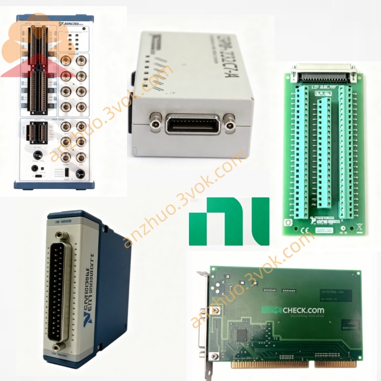
NI PXIe-2593 500MHz 16-CH 50Ω RF Multiplexer Switch
Description
Model Nomenclature
PXIe: PXI Express high‑speed modular instrumentation bus
25: NI switch/relay product series
93: 16‑channel, 50 Ω, 500 MHz RF multiplexer, latching EMR, MCX/SMB I/O
Technical Specifications
Form factor: 3U, 1‑slot PXIe (hybrid/peripheral slot compatible)
Topology: Software‑selectable—16×1 mux, dual 8×1 mux, dual 4×1 terminated mux, or sparse matrixNI
Relay type: Electromechanical latching (SPDT), silver‑palladium/gold contacts
Number of channels: 16 (signal) + 2 (trigger/COM)
Characteristic impedance: 50 Ω (nominal)NI
Bandwidth: DC to 500 MHzNI
Insertion loss: <0.9 dB (DC–200 MHz); <1.6 dB (200–500 MHz)
Isolation: >60 dB @ 500 MHz (channel‑to‑channel)
Maximum switching voltage: 150 VAC / 150 VDC (CAT I, channel‑to‑channel/ground)
Maximum switching current: 0.5 A (per channel)
Maximum RF carry power: 10 W (continuous, up to 500 MHz)
Minimum switch load: 10 mV / 10 μA
Operate time: Typical 2 ms; max 5 ms
Relay life: >5×10⁵ operations (rated RF conditions)
Triggering: PXI trigger lines 0–7; 2×SMB trigger/COM ports
Operating temperature: 0 °C to 55 °C; storage: −20 °C to 70 °C
Power consumption: 7 W @ 12 V, 3 W @ 3.3 V (PXIe)
Dimensions: 21.6 × 2.0 × 13.0 cm; weight: ~700 g
Interface and Communication Configuration
Front‑panel I/O: 18×MCX female (signal channels) + 2×SMB male (trigger/COM)
Bus: PXIe Gen1, plug‑and‑play (compatible with PXI hybrid slots)
Triggering: PXI trigger bus (0–7); SMB I/O for external triggering/synchronization
Software support: NI‑MAX for configuration; LabVIEW, LabWindows/CVI, C++ APIs with NI‑SWITCH driver; NI Switch Executive for advanced routingNI
Compatibility: Windows OS, 3U PXI/PXIe chassis
Core Features
500 MHz RF performance: Optimized for DC‑to‑500 MHz with low insertion loss and high isolation, ideal for RF and high‑speed digital signalsNI.
Flexible software‑configurable topologies: Adapts to 16×1, dual 8×1, dual 4×1 terminated, or sparse matrix without hardware changesNI.
Latching relay design: Maintains state without continuous power, reducing power draw and heat for long‑term reliability.
High RF power handling: Supports up to 10 W continuous RF power for robust signal routing in high‑power test applications.
Precision 50 Ω impedance matching: Ensures minimal signal reflection and optimal power transfer in RF systemsNI.
Deterministic scanning: Supports hardware‑timed scan sequences for repeatable automated test workflows.
Application Scenarios
Wireless device test: RF signal routing for 4G/5G modules, Bluetooth, Wi‑Fi, and IoT device validation.
Semiconductor RF test: Characterization of RF transistors, amplifiers, switches, and ICs in wafer probing and package test.
Aerospace & defense RF test: Signal switching for avionics, radar, and military communication systems up to 500 MHz.
High‑speed digital test: Routing high‑speed digital signals (up to 500 MHz) for PCB and assembly functional test.
RF ATE systems: High‑channel‑count RF routing for automated test equipment in manufacturing and validation labs.
Get a Quote