
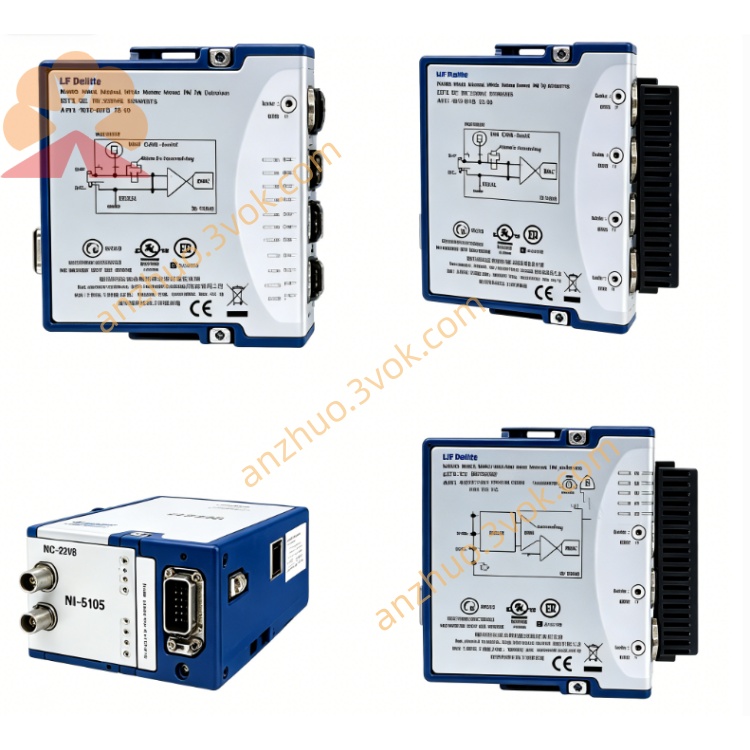
NI PXIe-2790 6GHz RF Power Combiner Switch Module
The PXIe-2790 is a solid-state RF combiner and switch module based on the PXI Express platform. Adopting CMOS solid-state switches, it operates across a frequency range from 10 MHz to 6 GHz. This module integrates signal routing and power combining functions, featuring ultra-fast switching speed and no mechanical wear. It is primarily designed for high-volume production test of cellular and wireless communication devices with multiple devices under test, delivering stable and reliable performance for long-term continuous operation.
Description
Model Nomenclature
PXIe refers to the PXI Express high-speed modular instrumentation bus. The number 27 stands for the series of RF switches and combiners. 2790 represents a power combining switch module with 6 GHz bandwidth and dual-channel combining architecture.
Technical Specifications
This module is a standard 3U single-slot unit, compatible with PXIe hybrid and peripheral slots. The nominal characteristic impedance is 50 ohms with AC coupling design. It uses CMOS solid-state switches with unlimited mechanical service life. The typical switching time is 45 microseconds. It supports PXI trigger lines numbered from 0 to 7 for synchronous control.
The module is configured with two channel groups and dedicated common ports, as well as a combined power output port. All external connections adopt SMA connectors on the front panel. Each independent channel and common port can handle a maximum continuous RF power of +20 dBm, while the combined output port supports up to +30 dBm continuous RF power. The maximum tolerable DC voltage is ±5 volts.
The operating temperature ranges from 0 degrees Celsius to 55 degrees Celsius, and the storage temperature ranges from -20 degrees Celsius to 70 degrees Celsius. The power consumption is approximately 1.2 watts on the 3.3 V power rail and up to 11 watts on the 12 V power rail.
Interface and Communication Configuration
The module applies the PXIe Gen1 bus and supports plug-and-play on Windows operating systems. All RF signal ports are equipped with SMA connectors for convenient cable connection. It supports two working modes including independent switching and scanning switching. Users can complete hardware configuration, parameter setting and status diagnosis via NI-MAX. Secondary development and program control are available through LabVIEW, LabWindows/CVI and C++ programming interfaces with the supporting driver. PXI trigger signals are used to realize synchronous switching between multiple modules.
Core Features
It provides wide frequency coverage from 10 MHz to 6 GHz, which is applicable to mainstream frequency bands of cellular communication, Wi-Fi and Bluetooth devices. The built-in power combining function enables two RF signal paths to combine power output, enhancing signal amplitude for test requirements. The solid-state switch structure eliminates mechanical abrasion and ensures long-term stable operation in high-frequency switching scenarios. All ports adopt 50 ohm impedance matching to reduce signal reflection and maintain excellent signal integrity. The fast switching capability effectively shortens test cycles and improves overall throughput of production test lines.
Application Scenarios
It is used for parallel production testing of multi-device cellular terminals, base station modules and wireless connectivity products. It conducts performance verification for RF components such as power amplifiers, filters and mixers. It serves as signal routing and power combining equipment in automated test systems for consumer electronics and automotive wireless modules. It is also widely applied to build multi-channel signal distribution and combined test platforms for general RF measurement systems.
Usage and Maintenance Instructions
Installation and Configuration
Insert the module into a 3U single-slot position of the PXIe chassis and fasten the front panel latch. Connect RF cables to corresponding SMA ports according to test requirements. Power on the chassis, and the system will automatically recognize the module. Open NI-MAX to configure working modes, channel connections and trigger parameters. Develop automated test programs via relevant programming tools to implement signal switching and power combining sequences.
Daily Maintenance
Place the module and chassis in a clean, dry and well-ventilated environment, and keep the ambient temperature within the rated range. Do not apply excessive force when plugging and unplugging SMA connectors to avoid damaging internal contacts. Check cables and connectors regularly for dirt, aging or poor contact. Ensure sufficient heat dissipation during long-time continuous operation. When the module is not in use, cut off the power, disconnect all cables and store it in a dry place with electrostatic protection.
Safety Notice
Do not input signals exceeding the rated RF power or DC voltage to prevent permanent damage to internal circuits. Follow electrostatic protection regulations when handling the module. Disconnect all power supplies of the chassis before installing, removing or maintaining the module. Dispose of the module in accordance with local electronic waste management regulations when it reaches the end of service life.
Get a Quote