
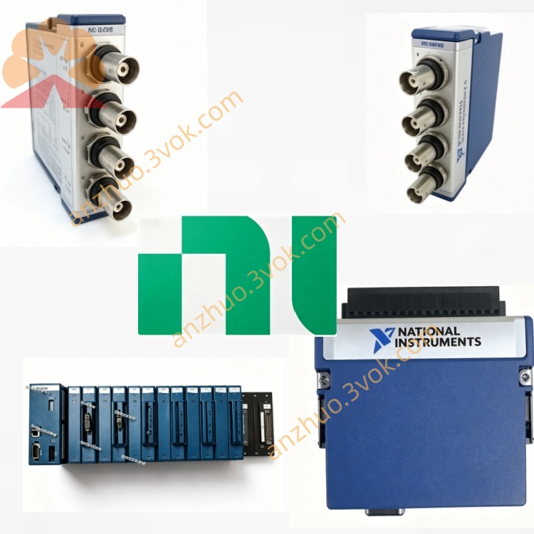
NI PXI‑5661 2.7‑GHz PXI RF Vector Signal Analyzer
Description
II. Model Interpretation
PXI: Compliant with the PXI industrial bus standard, 3U structure, occupying 2 slots, compatible with PXI and PXIe chassis.
5661: The serial number of the NI RF vector signal analyzer series, representing a 2.7GHz bandwidth model composed of a 5600 downconverter + 5142 digitizer, as an upgraded version of 5660.
Part Number: 778285-01 (32MB memory), 778285-02 (64MB memory).
III. Technical Specifications
Typical values under 25℃ environment, 50Ω load, preheating for 20 minutes
1 Frequency and Time Base
Operating frequency range: 9kHz to 2.7GHz
Real-time analysis bandwidth: 20MHz
Time base: 10MHz constant temperature crystal oscillator OCXO
Frequency stability: ±20ppb
Frequency accuracy: ±50ppb
Phase noise: At 1GHz carrier and 10kHz frequency offset, ≤ -129dBc/Hz at 10kHz
2 Input Power and Dynamic Range
Maximum input power: +30dBm
Input attenuation: 0 to 50dB, 10dB step NI
Spurious Free Dynamic Range: >80dB
Display Average Noise Level DANL: -165dBm/Hz
Input impedance: 50Ω
3 Digitization and Storage
Digitizer: PXI-5142, 14 bits
Sampling rate: 100MS/s
On-board memory: 32MB/64MB selectable
Digital Downconversion DDC: Supports 20MHz bandwidth IQ acquisition
4 Physical and Environmental
Specification: 3U, 2 slot
Power consumption: Approximately 28W
Operating temperature: 0℃ to 55℃
Heat dissipation: Forced air cooling of the chassis
IV. Interface and Communication Configuration
Front panel interface
PXI-5600 downconverter
RF IN: SMA female connector, 50Ω, RF signal input
10MHz OUT: SMA, output reference clock to 5142
POWER/STATUS: Power and lock-in status indicator lights
PXI-5142 digitizer
REF CLK IN: SMA, connect 10MHz reference clock
PFI: Programmable function interface, used for triggering and synchronization
Bus and Software
Bus: Standard PXI bus, including 32-bit PCI, trigger bus, 10MHz reference bus
Driver: NI-RFSA, supports LabVIEW, TestStand, Python, C#
Supporting software: Spectrum measurement toolkit, modulation analysis toolkit, supports frequency domain, IQ domain, demodulation measurement
V. Core Functions
1 Broadband signal analysis, covering the mainstream RF frequency band from 9kHz to 2.7GHz, 20MHz real-time bandwidth suitable for 2G/3G/4G, Bluetooth, Wi-Fi, etc. wireless signal acquisition.
2 High stability OCXO time base and low phase noise, ensuring frequency measurement accuracy and signal analysis reliability.
3 High-performance digitization and on-board DDC, 14-bit 100MS/s sampling, accurately capture IQ data, supporting complex modulation signal demodulation analysis.
4 Large dynamic range and high sensitivity, DANL as low as - 165dBm/Hz, capable of simultaneously measuring weak signals and strong signals.
4 Modular design, can be combined with PXI-5650 series signal generator to build a complete RF receive and transmit test system.
5 Flexible triggering and synchronization, supports frequency selectable burst triggering, suitable for communication and signal intelligent applications.
VI. Application Scenarios 1 Wireless communication testing, including 2G/3G/4G, Bluetooth, Wi-Fi, RFID devices' spectrum, modulation accuracy, adjacent channel power, and transmitter spurious emissions testing.
2 RF component testing, including gain, loss, linearity, harmonic and spurious emissions testing for amplifiers, filters, mixers, and RF switches.
3 Radar and electronic equipment testing, including mid-low frequency radar signal acquisition, RF environment simulation, and receiver sensitivity and anti-interference testing.
4 Aerospace and defense, including calibration of military RF equipment, RF link simulation, and RF sensor signal analysis.
5 Automotive electronics testing, including functionality and anti-interference testing of RF modules such as vehicle remote key, tire pressure monitoring, and vehicle Bluetooth.
VII. Installation and Maintenance Instructions
Installation and Power On
Power on after disassembly, with 5600 and 5142 fixed in adjacent slots, and the chassis reliably grounded for anti-static protection.
Preheat for 20 minutes, perform NI MAX self-check, confirm normal module operation and clock locking.
Keep the chassis ventilation duct unobstructed during operation, with the environmental temperature ≤ 55℃. Do not block the cooling fan.
Wiring and Operation
Connect RF IN with a 50Ω SMA cable, tighten the interface to reduce reflection loss, and avoid long-term input of overvoltage signals.
The 10MHz OUT of 5600 connects to REF CLK IN of 5142 to ensure module synchronization.
When synchronizing multiple devices, connect to an external 10MHz reference clock and enable the synchronization function.
Daily Maintenance and Calibration
Professional traceability calibration annually, use built-in self-calibration to correct temperature drift.
Regularly clean dust from SMA interfaces, keep them dry, and install dust caps when not in use.
Storage environment without condensation, humidity 10% to 90%, away from strong electromagnetic interference and vibration sources.
Do not power on while plugging or unplugging cables, avoid shock and vibration, and do not operate for long periods at excessive temperature.
Get a Quote