
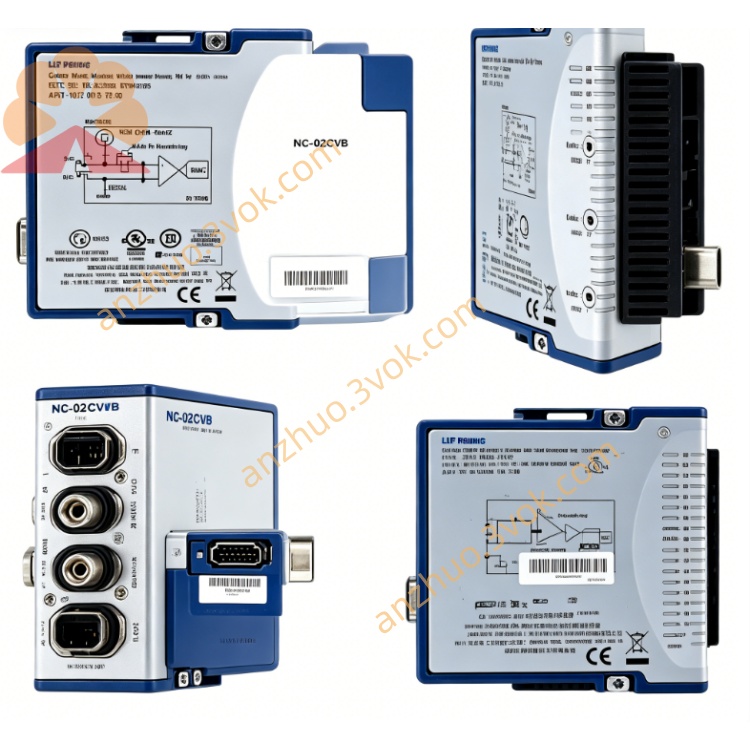
NI PXI-7952R Virtex-5 LX50 FlexRIO FPGA Module
Description
Basic Information
Model: PXI‑7952R (Part Number: 780561‑01)
Form Factor: 3U single‑slot PXI module
FPGA: Xilinx Virtex‑5 LX50
Onboard Memory: 128 MB DDR2 DRAM (two independent 64 MB banks)
I/O Channels: 132 single‑ended, configurable as 66 differential pairs
Programming Environment: LabVIEW FPGA, LabVIEW Real‑Time, Windows
Status: Discontinued; recommended replacement: PXIe‑7962R
Typical Power Consumption: ~5.5 W
Operating Temperature: 0 °C to 55 °C
Function and Positioning
Core Performance Parameters
FPGA Core
FPGA Model: Xilinx Virtex‑5 LX50
Logic Resources: 7,200 slices, 28,800 LUTs, 17,280 flip‑flops
Block RAM: 1,728 kbit (embedded)
DSP Slices: 48 DSP48 slices (18×18 multipliers)
Clock Speed: Default 40 MHz; FPGA internal up to 500 MHz; I/O up to 100 MHz
Configuration: LabVIEW FPGA, online reconfiguration supported
Digital I/O
Channel Configuration: 132 single‑ended / 66 differential pairs
I/O Standards: 1.2 V, 1.5 V, 1.8 V, 2.5 V, 3.3 V, LVDS, LVTTL, TTL
Max Rate: Single‑ended 100 MHz; differential 200 MHz
Functions: Input/output, counter/timer, PWM, encoder, custom protocols
Memory and Bus
Onboard DRAM: 128 MB DDR2 (64 MB × 2 banks), max bandwidth 6.4 GB/s
FIFO: 1,728 kbit block RAM
DMA: 3 DMA channels, 32 DMA interrupt channels; PXI bus up to 400 MB/s
Synchronization: PXI trigger bus, RTSI; sync accuracy <25 ns
Physical and Electrical
Dimensions: 3U (160 mm × 100 mm)
Connector: 1 × dedicated FlexRIO adapter interface
Power: +3.3 V, +5 V from PXI backplane
Weight: ~190 g
Compatible Accessories
FlexRIO Adapter Modules
NI‑6581: High‑speed digital I/O adapter, 100 MHz, 132 channels
NI‑5781: Analog input/output adapter, high‑speed signal acquisition/generation
NI‑5751: 16‑channel digitizer adapter, 50 MS/s, 14‑bit
NI FlexRIO Adapter MDK: Development kit for custom adapter design
Software
NI‑FlexRIO Driver: Hardware configuration, FPGA programming, DMA management
LabVIEW FPGA Module: Graphical FPGA development, real‑time logic design
LabVIEW Real‑Time: Deterministic control and data processing
Application Fields
High‑Speed Digital Test Systems: Functional verification of digital circuits, high‑speed pulse generation/acquisition, custom digital bus emulation.
Real‑Time Signal Processing: Digital filtering, FFT analysis, sensor data preprocessing, hardware‑in‑the‑loop (HIL) simulation.
Industrial Automation and Control: Multi‑axis motion control, encoder signal decoding, high‑speed PWM control, custom protocol conversion.
Aerospace and Defense: Radar signal processing, communication protocol analysis, avionics testing, high‑speed data logging.
Scientific Research and Instrumentation: FPGA‑based prototype development, physics experiment control, high‑speed data acquisition.
Semiconductor Test: Wafer testing, digital IC validation, high‑speed interface testing.
Get a Quote