
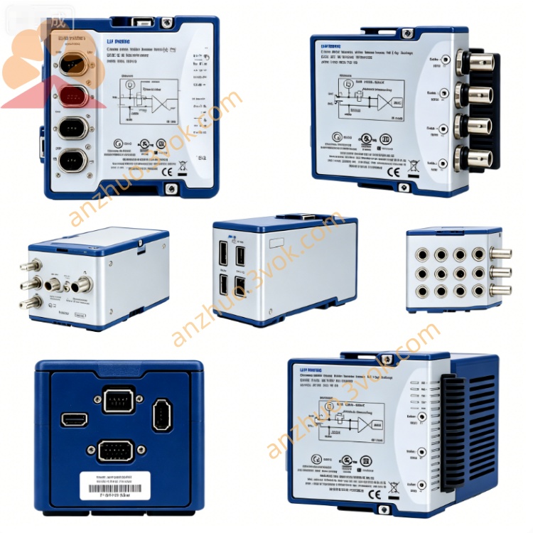
NI PXI-7951R Virtex-5 LX30 FlexRIO FPGA Module
Description
II. Model Interpretation
PXI: Standard 3U single-slot structure, using the traditional PXI bus, compatible with conventional PXI/PXIe chassis slots.
7951R: Belongs to the FlexRIO series. The digit 5 indicates the use of the fifth-generation Virtex-5 architecture FPGA; the digit 1 represents the basic configuration, using the LX30 chip and without onboard DRAM; the suffix R indicates reconfigurable I/O, with user-programmable FPGA onboard.
Product Positioning: Low-cost FPGA carrier board, targeting basic reconfigurable computing and high-speed digital interface development scenarios.
III. Technical Parameters (25℃ Ambient Temperature Environment)
1. FPGA Core Parameters
Chip Model: Xilinx Virtex-5 LX30
Logic Resources: 4800 logic units, trigger, distributed storage resources meet the requirements for small-scale logic design
Computational Resources: Built-in 32 18×18 hardware multipliers, supporting basic digital signal operations
Clock Performance: Board default 40 MHz base clock; FPGA internal maximum operating frequency 500 MHz, I/O interface maximum clock 100 MHz
Programming Method: Supports LabVIEW FPGA graphical programming, can be reconfigured online for logic programs
2. General I/O and Electrical Characteristics
Channel Specifications: Total 132 single-ended channels, can be flexibly configured as 66 differential channels
Voltage Standards: Supports 1.2 V, 1.5 V, 1.8 V, 2.5 V, 3.3 V, compatible with LVDS, LVTTL, TTL multiple electrical specifications
Transmission Rate: Single-ended signal maximum 100 MHz, differential signal maximum 200 MHz
Channel Functions: Can be configured as general input, output, counter, timer, PWM, quadrature encoder interface, supports custom communication protocols
3. Storage and Bus Transmission
Onboard Storage: No independent DRAM, only uses FPGA internal block RAM, can cache 128 KB
Bus Specifications: PXI standard bus, peak transmission bandwidth 400 MB/s
DMA Channels: Equipped with 3 sets of DMA transmission channels and 32 DMA interrupts, achieving high-speed data flow
Synchronization Capability: Supports PXI trigger bus, RTSI real-time synchronization bus, multi-module synchronization error less than 25 ns
4. Physical and Environmental Parameters
Form Specification: 3U single-slot PXI module
External Interfaces: Single dedicated FlexRIO adapter interface for connecting front-end I/O modules
Power Supply Requirements: Backplane + 3.3 V, +5 V power supply, typical module power consumption 4.5 W
Operating Temperature: 0 ℃ ~ 55 ℃
Storage Temperature: -20 ℃ ~ 70 ℃ IV. Interface and Communication Configuration
1. Hardware Interfaces
Adapter Interface: Special high-density connector, used for connecting NI-6581 digital adapter, NI-5781 analog adapter, etc. to the front-end modules, expanding analog, digital, and RF functions.
Backplane Bus of the Cabinet: Connects to the local PXI bus, 8-channel PXI trigger bus, RTSI synchronization bus, and is compatible with the standard 10 MHz reference clock of the cabinet.
External Clock: Supports external 10 MHz to 100 MHz clock signals, which can be aligned with the external instrument timing.
2. Software and Drivers
Companion Driver: NI-FlexRIO, responsible for hardware identification, FPGA configuration, channel and bus management.
Development Environment: Compatible with LabVIEW FPGA, LabVIEW Real-Time, and conventional Windows system development environments.
Development Process: Completes hardware logic programming, compilation, and download to the onboard chip on the FPGA end; The upper computer or real-time system completes data interaction through DMA, registers, and FPGA.
Protocol Support: Can independently implement SPI, I2C, UART, parallel bus, and various customized communication protocols.
V. Core Functions
Multilevel High-Speed Digital Interface
132 channels support single-ended and differential modes, compatible with various industrial and high-speed digital level standards, meeting requirements for high-speed pulse transmission, encoder signal acquisition, bus communication, etc.
High Performance Reconfigurable FPGA Computing
Virtex-5 LX30 chip with a maximum internal clock of 500 MHz can independently run timing logic, state machines, basic digital algorithms, without operating system delay, achieving hard real-time control.
Modular Flexible Expansion
Based on the standard FlexRIO adapter interface, can be combined with different front-end modules as needed, quickly build pure digital, mixed-signal, RF, etc. systems with strong hardware expansion capability.
Multi-device Precise Synchronization
Utilizing the PXI trigger bus and RTSI bus, achieve nanosecond-level timing synchronization between multiple FlexRIO modules and multiple cabinets, suitable for large parallel test systems.
High-Speed Data Transmission
Multiple DMA channels combined with high-bandwidth PXI bus, realize continuous transmission of large-capacity data, ensuring data integrity in high-speed acquisition and signal playback scenarios.
VI. Application Scenarios
High-Speed Digital Testing System
Function verification of digital circuit boards, high-speed pulse signal generation and acquisition, custom digital bus simulation.
Hardware Prototype Development
Quick prototype verification of small-scale digital circuits, dedicated control logic, communication protocols for rapid development of hardware.
Industrial Automation Control
Analysis of multi-axis motion encoder signals, high-speed PWM control, custom interface conversion between devices.
Real-time Signal Processing
Simple digital filtering, timing judgment, basic arithmetic real-time processing scenarios.
Teaching and Research Platform
FPGA principle teaching, reconfigurable technology experiments, basic digital signal processing research.
VII. Usage and Maintenance Instructions
1. Installation and Power On
When the power is off, insert the module into the PXI cabinet slot, tighten the fixing screws to ensure the cabinet is reliably grounded. Before powering on, check that the adapter connection is secure and prohibit short-circuiting of interface pins without power. During equipment operation, keep the cabinet ventilated to avoid temperature accumulation affecting the stability of the clock and logic.
2. Wiring and Operation
Use the original factory-compatible adapter and shielded cable, distinguish between digital and analog signal wiring to reduce signal crosstalk. Single-ended cable length should be within 3 meters, and differential cable length should not exceed 10 meters. The hardware identification and basic configuration are completed through NI MAX. During the compilation of the FPGA program, strict adherence to clock constraints is required. When using for the first time, the channel function is tested without load. Once it is normal, external loads and devices are connected.
3. Daily Maintenance
Regularly check the interface and cable connection status of the adapter, clean the dust on the interface surface, and install dust caps on the interface when it is idle for a long time to prevent oxidation and poor contact. The module is a pure digital circuit and does not require frequent calibration. It is recommended to conduct an overall function inspection once a year. Regularly update the NI-FlexRIO driver and FPGA firmware to improve compatibility and operational stability.
Get a Quote