
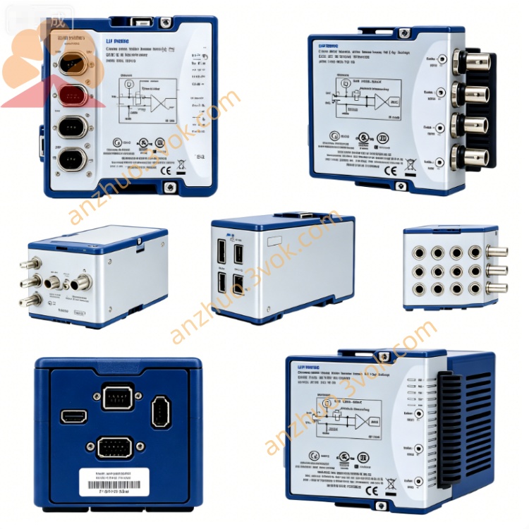
NI PXI-7954R FlexRIO Virtex-5 LX110 FPGA Reconfigurable PXI Module
Description
Model Nomenclature
PXI: Compliant with the PXI (PCI eXtensions for Instrumentation) modular instrumentation bus standard.
7954: Series identifier; 795x denotes the first‑generation FlexRIO FPGA carrier family, and 4 indicates the highest performance level in the series.
R: Reconfigurable, signifying a user‑programmable FPGA on board.
Full meaning: PXI bus, 795x series, highest performance, reconfigurable FPGA carrier module.
Technical Specifications
Form factor: 3U single‑slot PXI module.
Part number: 780563‑01.
FPGA: Xilinx Virtex‑5 LX110.
Onboard memory: 128 MB DDR2 (64 MB × 2), 6.4 GB/s bandwidth.
Block RAM: 4,608 kbit.
DSP slices: 64 DSP48 (18×18 multipliers).
Logic resources: 17,280 slices, 69,120 LUTs, 41,472 flip‑flops.
Power consumption: Approximately 7.5 W.
Operating temperature: 0 °C to 55 °C.
Storage temperature: −40 °C to 71 °C.
Channels: 132 single‑ended / 66 differential pairs.
Logic levels: 1.2 V, 1.5 V, 1.8 V, 2.5 V, 3.3 V, LVDS, LVTTL, TTL.
Maximum rate: 100 MHz single‑ended, 200 MHz differential; PXI bus up to 400 MB/s.
Functions: Input/output, counter/timer, PWM, encoder, custom protocols, high‑speed streaming.
Default system clock: 40 MHz.
Maximum FPGA internal clock: 500 MHz.
Synchronization interfaces: PXI trigger bus, RTSI; multi‑module synchronization accuracy < 25 ns.
Bus interface: PXI (PCI).
DMA: 3 DMA channels, 32 DMA interrupt channels.
Data transfer: DMA, interrupts, programmed I/O.
Interface and Communication Configuration
1 dedicated FlexRIO adapter interface (for connecting NI‑6581, 5761, 5781, 5791, and other front‑end modules)NI.
PXI backplane: +3.3 V, +5 V power supply, PXI trigger bus, RTSI synchronization bus.
Drivers: NI‑FlexRIO, NI‑RIO.
Programming environments: LabVIEW FPGA (graphical), LabVIEW Real‑Time, Windows; mixed‑language support with VHDL.
Operating systems: Windows 7/10, LabVIEW Real‑Time.
Core Features
- User‑defined FPGA hardware logicBased on the Virtex‑5 LX110, it enables parallel processing, custom timing, proprietary protocols, and high‑speed control that runs independently of the CPU with hard real‑time performance.
- High‑density, high‑speed digital I/O control132 configurable channels supporting 100 MHz single‑ended / 200 MHz differential operation, ideal for high‑speed digital test, bus emulation, encoder and motion control interfaces.
- Real‑time signal processing and high throughput64 DSP slices plus 128 MB high‑bandwidth memory support FFT, filtering, demodulation, multi‑sensor fusion, and HIL simulation; PXI bus at 400 MB/s enables DMA‑based high‑speed data streaming.
- Modular expansion and software‑defined instrumentationWhen combined with FlexRIO adapters, it rapidly builds high‑speed digitizers, arbitrary waveform generators, RF transceivers, and parallel digital test systemsNI.
- Precision multi‑module synchronizationUsing the PXI trigger and RTSI buses, it achieves nanosecond‑level synchronization across multiple cards, suitable for multi‑channel parallel test and distributed data acquisition.
Applications
- Semiconductor testHigh‑speed IC validation, SoC interface test, memory test, and parallel wafer probe test.
- Radar, communications, and RF testRadar signal processing, 5G/LTE protocol decoding, RF transceiver test, and software‑defined radio (SDR).
- Aerospace and defenseAvionics full‑interface test, satellite communication signal processing, high‑speed flight data recording, and electronic warfare (EW) analysis.
- Industrial automation and motion controlMulti‑axis (10+ axis) high‑speed motion control, complex encoder processing, hardware implementation of industrial Ethernet (EtherCAT/PROFINET), and high‑speed machine vision integration.
- Research and precision measurementHigh‑energy physics experiment control, high‑speed imaging data processing, custom scientific instruments, and large‑scale parallel data acquisition.
Usage and Maintenance
Install only in a standard 3U PXI/PXIe chassis using dedicated rails and locking mechanisms.
Power is supplied exclusively from the PXI backplane; do not use external power. Verify chassis power capacity (≥10 W per slot) before power‑on.
Install FlexRIO adapters only when power is off; align guides and insert evenly, then lock.
Required software: LabVIEW, LabVIEW FPGA Module, NI‑FlexRIO, NI‑RIO drivers.
FPGA logic is compiled and downloaded via LabVIEW FPGA, supporting online reconfiguration without power‑off.
For high‑speed I/O and DMA transfers, implement timing constraints and buffer design in the FPGA to avoid data loss.
Operating temperature: 0 °C to 55 °C. Ensure chassis fans operate normally and airflow is unobstructed; derate in high‑temperature environments.
Humidity: 10% to 90% RH, non‑condensing. Avoid dust, corrosive gases, and strong electromagnetic interference.
Periodically clean chassis filters and module gold fingers (power off, use anhydrous alcohol).
Driver issues: Reinstall NI‑FlexRIO/NI‑RIO drivers and restart; do not mix driver versions.
FPGA load failures: Check adapter connection, recompile BIT file, verify stable chassis power.
Long‑term storage: Power off and store in a dry environment; power on for 1 hour monthly to prevent moisture damage.
For indoor industrial/test environments only, altitude ≤2000 m, pollution degree 2.
Dispose of in accordance with electronic waste regulations; do not discard improperly.
Get a Quote