
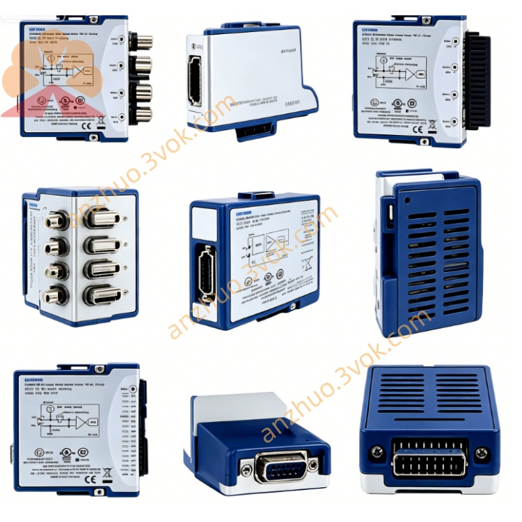
NI PXI-7852R Virtex-5 LX50 Multifunction RIO FPGA Module
Description
II. Model Interpretation
PXI: 3U single slot, PXI Hybrid bus, compatible with PXI/PXIe
7852: Fifth generation (Virtex-5) mixed RIO; 5 = Fifth generation FPGA; 2 = 8AI + 8AO + 96DIO configuration
R: Reconfigurable I/O (reconfigurable I/O), onboard user-programmable FPGA
III. Technical Parameters (25℃)
1) FPGA Core
Model: Xilinx Virtex-5 LX50 (LX50 = 50K logic units)
Logic Resources: 48,000 flip-flops, 2,880 kbit block RAM, 64 18×18 multipliers
Clock: Maximum 200 MHz; I/O clock 40 MHz
Configuration: LabVIEW FPGA, supports online reconfiguration, partial reconfiguration
2) Analog Input (AI)
Channels: 8 single-ended / differential selectable
Resolution: 16 bits
Sampling Rate: Each channel independently 750 kS/s (multi-channel synchronous)
Voltage Range: ±10 V
Bandwidth: 300 kHz
Trigger: Independent trigger (level / window / slope) for each channel
3) Analog Output (AO)
Channels: 8 single-ended
Resolution: 16 bits
Update Rate: Each channel independently 1 MS/s
Voltage Range: ±10 V
Drive Capacity: ±5 mA
Setup Time: 10 μs (to ±0.01%)
4) Digital I/O (DIO)
Channels: 96 bidirectional TTL/CMOS, groupable
Rate: Maximum 40 MHz, supports bilateral edge sampling
Level: 3.3 V/5 V compatible, each channel drives 24 mA
Functions: Input / Output / Counter / PWM / Encoder / Custom Protocol
5) Memory and Bus
Onboard RAM: 256 KB (FPGA block RAM)
FIFO: AI 64 KB, AO 64 KB, DIO 32 KB
DMA: 3 channels, maximum 132 MB/s on PXI bus
Trigger: PXI trigger bus, RTSI, star trigger, synchronous **<25 ns**
6) Physical and Environmental
Size: 3U single slot (160 mm × 100 mm)
Connectors: 2×68-pin VHDCI (1 AI/AO, 1 DIO)
Power Supply: +3.3 V (1.8 A), +5 V (20 mA); Power consumption approximately 5 W
Temperature: 0 ℃ ~ 55 ℃ (standard); optional **−40 ℃ ~ 85 ℃**
Weight: Approximately 180 g
IV. Interface and Communication Configuration
1) Hardware Interface
Analog I/O: 68-pin VHDCI (J1), 8AI/8AO, differential support
Digital I/O: 68-pin VHDCI (J2), 96DIO, divided into 3 groups × 32 channels
Backplane: PXI local bus, trigger bus, RTSI, PXI_CLK10 (10 MHz)
Clock: Internal 40 MHz; supports external 10–40 MHz input, PXIe reference clock
2) Software and Drivers
Driver: NI-RIO, compatible with LabVIEW FPGA, Real-Time, Windows
Development Process:
FPGA side: Graphical programming of acquisition / control / protocol logic
Real-time / Host side: DMA transmission, data processing, upper computer interaction Supporting protocols: SPI, I2C, UART, CAN, custom parallel bus
VII. Core Functions
Integrated mixed-signal (8AI + 8AO + 96DIO)
Single-card synchronous implementation of analog acquisition, signal generation, and high-speed digital control, eliminating the need for multiple module wiring, suitable for compact systems.
Virtex-5 FPGA hard real-time processing (25 ns accuracy)
Board-mounted FPGA operates independently for closed-loop control, sequential logic, protocol parsing, without operating system delay, supporting microsecond-level HIL closed-loop.
Multiple-rate independent channels (750 kS/s AI, 1 MS/s AO)
Each channel can independently sample / update rate, independently trigger, supporting multi-rate mixed acquisition, suitable for complex signal scenarios.
96-channel high-speed DIO (40 MHz)
Can be configured as encoder interface, PWM output, high-speed pulse string, custom protocol, suitable for motion control, digital communication.
Precise synchronization and high-bandwidth transmission
Supports PXI trigger / RTSI / star trigger, multi-card synchronization < 25 ns; DMA streaming transmission, meeting high-speed continuous acquisition / generation requirements.
VI. Application Scenarios
Hardware-in-the-Loop (HIL) real-time simulation
Motor / inverter HIL, power electronics simulation, power supply control testing, microsecond-level closed-loop.
Industrial control and motion control
Multi-axis synchronous motion (encoder + pulse instructions), high-speed sorting line, custom PLC substitution, analog + digital interlock.
High-speed mixed-signal testing
Sensor array acquisition, analog circuit function verification, high-speed pulse testing, 16-bit high-precision signal generation.
Custom protocols and interface conversion
Military / aviation dedicated protocols, old equipment interface adaptation, SPI/I2C/CAN etc. protocol hardware implementation.
Research and equipment development
Laser control, ultrasonic testing, precise motion control, real-time signal processing prototype verification.
VII. Usage and Maintenance Instructions
1) Installation and Power On
Disconnect power, insert a single slot of the PXI/PXIe chassis, tighten the fixing screws, and ensure the chassis is reliably grounded.
Before powering on, check that the VHDCI cables have no short circuit / false connection, and separate the analog / digital cables for wiring.
Preheat for 15 minutes before performing precise tests to ensure stable timing and accuracy.
2) Wiring and Configuration
Cables: Shielded VHDCI cables, analog signals use differential lines, digital lines length ≤ 3 m.
Configuration: NI MAX recognizes the hardware; LabVIEW FPGA compilation clock constraint ≤ 40 MHz.
Debugging: First test the basic functions of AI/AO/DIO without load, then connect the load; Use FPGA probe to monitor signals in real time.
3) Daily Maintenance
Regularly clean the VHDCI connector, check the shielding layer, add a dust cap for long-term inactivity.
Calibration: Once a year, use NI calibration tools to verify the accuracy of AI/AO and DIO timing.
Firmware: Update NI-RIO driver and FPGA firmware to optimize performance and compatibility.
Get a Quote