
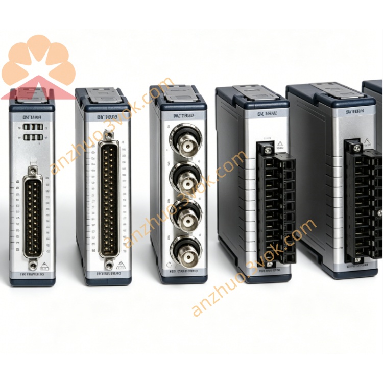
NI PXI‑5650 1.3‑GHz PXI RF Analog Signal Generator
Description
II. Model Interpretation
PXI represents that the equipment follows the PXI industrial bus standard and adopts a 3U structure, occupying a single cabinet slot, and is compatible with both PXI and PXIe cabinets.
5650 belongs to the NI 5650 series of RF signal generators. This series is a general-purpose RF analog signal source product line. The digital number distinguishes the frequency ranges. 5650 corresponds to the highest working frequency of 1.3 GHz version.
The standard complete unit part number is 778284-01.
III. Technical Parameters
All of these parameters are typical values under a 25-degree Celsius environment and a 50-ohm standard load.
1. Frequency Parameters
Operating frequency range: 50 kHz to 1.3 GHz. The signal can be probed down to 100 kHz. There are no calibration indicators in this range.
Frequency resolution: less than 1 Hz
Frequency annual stability: plus or minus 0.1 ppm
Phase noise: at 100 MHz carrier, 1 kHz frequency offset is less than -125 dB/Hz at 1 GHz carrier, 10 kHz frequency offset is less than -105 dB/Hz
2. Output Power Parameters
50 kHz to 10 MHz range: power range from -90 dBmW to 5 dBmW
10 MHz to 50 MHz range: power range from -90 dBmW to 8 dBmW
50 MHz to 1.3 GHz range: power range from -90 dBmW to 10 dBmW
Power resolution: less than 0.1 dB
Power typical accuracy: plus or minus 0.5 dB
3. Modulation Parameters
Supports frequency modulation function. Maximum frequency offset: plus or minus 1 MHz
Supports dual-frequency shift keying function. Frequency offset can be programmed by software
Supports on-off keying function. Achieves amplitude on-off control
4. Interference and Harmonic Parameters
Harmonic components: typical value less than -15 dB carrier
Non-harmonic stray signals: typical value less than -60 dB carrier
5. Physical and Environmental Parameters
Equipment specification: 3U single-slot structure
Overall power consumption: approximately 15 watts
Operating temperature range: 0 degrees Celsius to 55 degrees Celsius
Cooling method: cabinet forced air cooling
IV. Interface and Communication Configuration
Front panel interface
RF output interface: uses SMA interface, standard impedance 50 ohms, used for output RF signal
Reference clock input interface: uses SMA interface, connects to a 10 MHz external reference clock to achieve multi-device synchronization
Bus and software configuration
The device backplane is equipped with a standard PXI bus, including 32-bit PCI bus, PXI trigger bus, and 10 MHz reference bus, supporting signal triggering and clock sharing between devices.
The accompanying driver program is NI-RFSG, which can be used in development environments such as LabVIEW TestStand Python C#.
Supports NI-TClk synchronization technology, enabling phase synchronization of multiple modules.
V. Core Functions
1. Wideband continuous wave output, covering mainstream very high frequency, extremely high frequency, and cellular low frequency band signals, meeting the requirements of conventional RF frequencies.
2. Built-in high-stability constant temperature crystal oscillator, strong frequency stability, excellent phase noise indicators, ensuring RF measurement accuracy.
3. Integrated multiple basic modulation functions, can directly output frequency modulation, frequency shift keying, and on-off keying signals, without the need to additionally pair with baseband modules.
4. Equipped with automatic level control function, output power is stable, can weaken the influence of temperature changes and load fluctuations.
5. Standard PXI modular design, can be used in conjunction with the same platform RF acquisition, analysis modules to build a complete automated RF test system.
6. Large power adjustment range, can output small signals and conventional power signals, suitable for different test scenarios.
VI. Application Scenarios 1. Wireless communication testing, used for the receiver sensitivity and anti-interference capability tests of second-generation, third-generation, fourth-generation mobile communication devices, wireless local area networks, Bluetooth, and low-power wireless devices.
2. RF component testing, completing the gain loss and linearity detection of RF amplifiers, filters, mixers, RF switches and other devices.
3. Radar and electronic equipment testing, outputting basic continuous waves and modulated RF signals, simulating simple radar excitation signals and RF environment.
4. Aerospace and defense field, used for the calibration of military RF equipment, RF link simulation and the excitation of various RF sensor signals.
5. Automotive electronics testing, conducting functional and anti-interference tests for RF modules such as vehicle remote key, tire pressure monitoring, and vehicle Bluetooth.
Seven. Installation and Maintenance Instructions
Installation and Power On
The equipment must be installed in the power-off state, fixed in a single slot of the PXI chassis, and the chassis should be reliably grounded to prevent static damage to the hardware.
After installation, power on the equipment, preheat for thirty minutes to ensure that the internal constant temperature crystal oscillator reaches a stable working state. Use the NI MAX software to complete the equipment self-check and confirm no hardware faults.
During the operation of the equipment, ensure that the air duct of the chassis is unobstructed, the working environment temperature does not exceed 55 degrees Celsius, and do not block the chassis cooling fan.
Cable Connection and Operation
The RF output terminal uses a 50-ohm standard SMA coaxial cable for connection, tighten the interface to reduce signal reflection and loss.
It is not recommended to short-circuit the RF output interface for a long time for grounding, to avoid damaging the final amplification circuit of the equipment. Preferably use a 50-ohm matching load.
When working synchronously with multiple devices, uniformly connect to an external 10 MHz reference clock, enable the synchronization function, and ensure that the phases of all devices are consistent.
Daily Maintenance and Calibration
It is recommended to conduct a professional trace calibration once a year to compensate for the parameter offset caused by long-term use of the equipment. Daily use can use the built-in self-calibration function of the equipment to correct the performance changes caused by temperature.
Regularly use a drying tool to clean the dust on the SMA interface surface to keep the interface dry and clean. When the equipment is idle for a long time, install a dust cap on the interface.
The equipment storage and usage environment should be free of condensation, with the humidity controlled between 10% and 90%. Stay away from strong electromagnetic interference equipment and severe vibration sources.
Do not plug or unplug the signal cables while the equipment is powered on to avoid the equipment being impacted and subjected to severe vibration. Do not operate for a long time in an environment exceeding the rated temperature.
Get a Quote