
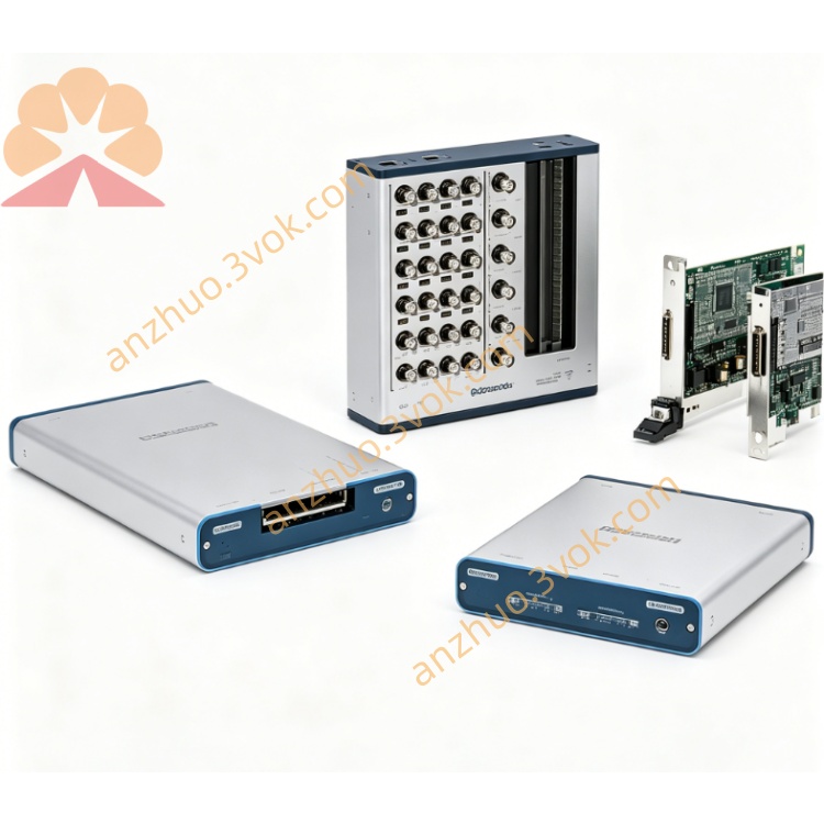
NI PXI‑5600 2.7‑GHz PXI RF Down‑Converter
Description
II. Model Interpretation
PXI: Standard 3U PXI bus, single slot, compatible with PXI/PXIe chassis.
5600: NI 5600 series RF downconverter model number:
56xx: RF/microwave instrument series;
xx00: Basic broadband downconverter (without integrated digital instrument).
Component number: 778283-01 (standard configuration, unique model).
Combination model: PXI-5600 + PXI-5142 = PXI-5661 VSA.
III. Technical Parameters (25℃, 50 Ω, typical values)
1. Frequency and Bandwidth
RF input frequency: 9 kHz – 2.7 GHz
Real-time bandwidth: 20 MHz (fixed IF bandwidth)
Output intermediate frequency (IF): 5 – 25 MHz
2. Input/Output Characteristics
RF input: SMA female, 50 Ω, AC coupling
Maximum input power: +30 dBm
Attenuation: 0 – 50 dB (10 dB step)
Noise density: < -135 dBm/Hz
IF output: SMA female, 50 Ω, 0 dBm full scale
3. Time Base and Stability
Reference source: Built-in 10 MHz OCXO (highly stable constant-temperature crystal oscillator)
Frequency stability: ±20 ppb (annual)
Frequency accuracy: ±50 ppb
Phase noise: < -94 dBc/Hz @ 10 kHz offset (1 GHz carrier)
4. Dynamic Range and Spurious
Spurious-free dynamic range (SFDR): > 80 dB
Third-order intermodulation: > 70 dBc
5. Physical and Environmental
Size: 3U single slot (approximately 160×100 mm)
Power consumption: approximately 18 W
Operating temperature: 0 – 55℃
Cooling: Forced air cooling (chassis fan)
IV. Interface and Communication Configuration
1. Front Panel (3×SMA)
RF IN (SMA): RF signal input, 50 Ω, AC coupling
IF OUT (SMA): Intermediate frequency output after downconversion, connected to PXI-5142's IF IN
REF IN (SMA): 10 MHz external reference input (-5 to +15 dBm), used for multi-card synchronization
2. Backplane and System Interface
PXI backplane: 32-bit PCI, PXI trigger bus (TRIG0–TRIG6), 10 MHz reference bus
Synchronization: Supports PXI trigger, NI-TClk multi-module phase synchronization
Driver: NI-RFSA (RF vector signal analysis driver), compatible with LabVIEW/TestStand/Python/C#
V. Core Functions
Broadband RF downconversion: 9 kHz – 2.7 GHz → 5 – 25 MHz IF, 20 MHz real-time bandwidth, covering mainstream wireless/radar frequency bands.
Highly stable OCXO time base: ±20 ppb stability, low phase noise, ensuring precise frequency and modulation measurement.
Large dynamic range: +30 dBm full scale, < -135 dBm/Hz noise density, > 80 dB SFDR, suitable for scenarios with both strong and weak signals.
Modular combination: Seamless integration with PXI-5142 (14-bit/100 MS/s digital instrument), quickly building PXI-5661 VSA.
Multi-card synchronization: Shared 10 MHz reference + NI-TClk, multi-module synchronization accuracy < 20 ps, supporting MIMO/multi-channel RF testing. VI. Application Scenarios
Wireless communication testing: 2G/3G/4G/5G (Sub-6G), WiFi, Bluetooth signal reception and demodulation, receiver sensitivity / anti-interference testing.
Radar / Electronic Warfare: Intermediate frequency acquisition in radar, pulse train / LFM signal analysis, electronic countermeasures (ECM) signal monitoring.
Aerospace / Defense: Low spurious RF reception, sensor simulation, military RF equipment calibration and verification.
Semiconductor testing: RF amplifier / filter / mixer performance verification, transceiver chip (SoC) modulation accuracy testing.
General RF R&D: Broadband signal capture, spectrum analysis, modulation quality (EVM / phase error) measurement.
VII. Usage and Maintenance Instructions
1. Installation and Power On
Power off installation, single slot fixed; chassis reliable grounding to prevent static electricity.
Power on preheating for 30 minutes (OCXO requires stable temperature), NI MAX self-check without hardware errors.
Keep ventilation during operation, temperature ≤ 55℃, avoid blocking the chassis fan.
2. Wiring and Operation
RF input uses 50 Ω high-precision SMA coaxial cable, tighten the connector, reduce standing wave.
Input power must not exceed + 30 dBm, otherwise burn the front end; strong signals (> 0 dBm) must be attenuated.
Multi-card synchronization: share 10 MHz reference (REF IN), enable NI-TClk, ensure phase coherence.
3. Calibration and Maintenance
Calibration cycle: recommended 1-year NIST traceable calibration; daily use internal self-calibration to compensate for temperature drift.
Interface maintenance: regularly clean SMA interface, keep dry; install dust cover for long-term inactivity.
Environmental requirements: no condensation, humidity 10%–90% RH; away from strong electromagnetic interference and vibration sources.
Prohibited operations: plug and unplug cables while powered on, overheating operation, interface overload, severe vibration.
Get a Quote