
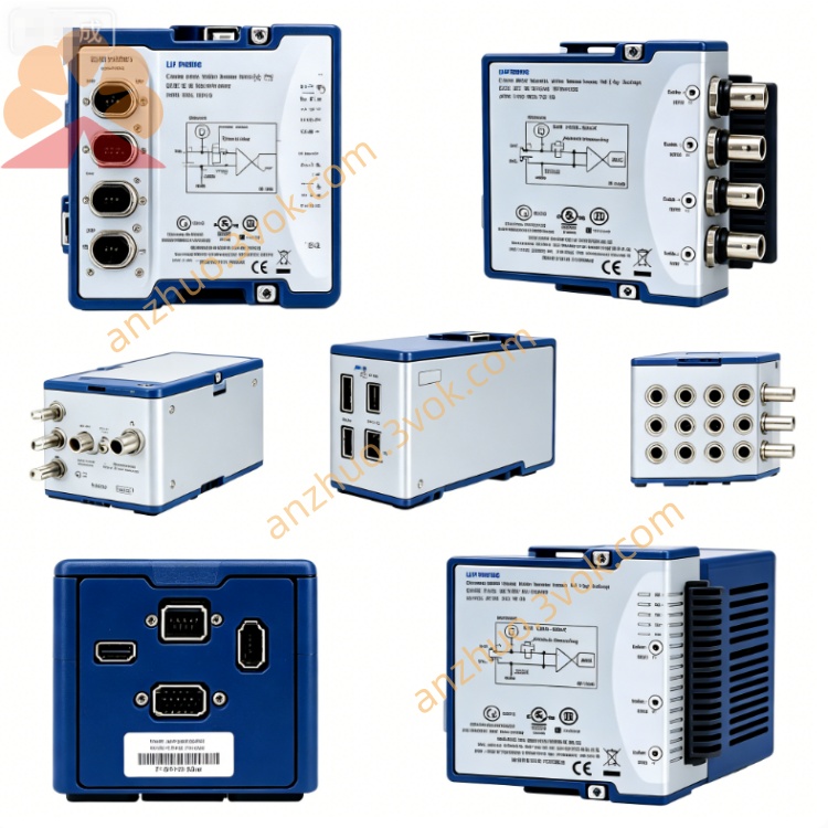
NI PXI‑5412 40 MS/s Arbitrary Waveform Generator
Description
II. Model Interpretation
PXI: 3U PXI standard bus, single slot, compatible with PXI/PXIe chassis.
5412: NI 5400 series high-performance arbitrary waveform generator:
54xx: Arbitrary waveform / function generator series
x4x: Analog output, medium-high bandwidth
xx12: 1 channel, 14 bits, 100 MS/s, 20 MHz bandwidth basic high-performance version
Component number: 778577-01 (standard configuration for PXI-5412).
III. Technical Parameters (25℃, 50 Ω terminal, typical values)
1. Basic Performance
Channel number: 1 analog output
Resolution: 14-bit DAC
Sampling rate: 100 MS/s; equivalent to 400 MS/s after 8 times interpolation
Bandwidth (–3 dB): 20 MHz (sine / square wave)
Output amplitude: 12 Vpp (±6 V) @ 50 Ω; software adjustable from 5.64 mVpp to 12 Vpp (NI)
Output impedance: 50 Ω/75 Ω (software selectable)
Frequency resolution: 1.06 μHz (DDS, continuous phase)
2. Frequency Upper Limit (typical)
Sine: 20 MHz
Square wave: 5 MHz
Triangle / Sawtooth: 1 MHz
3. Storage and Synchronization
Waveform memory: 8/32/256 MB (optional, SMC shared memory)
Synchronization accuracy: <20 ps RMS skew between multiple modules (NI-TClk)
Trigger / Clock: PXI trigger bus, REF IN/OUT (10 MHz), PFI
4. Environment and Power Consumption
Operating temperature: 0~55℃ (NI)
Power consumption: approximately 22 W
Size: 3U single slot (approx. 160×100 mm)
IV. Interface and Communication Configuration
Front panel (single-slot cover, 4×SMB)
CH0 (SMB): Analog output, 50/75 Ω selectable, ±6 VmaxNI
REF IN (SMB): External reference clock input (10 MHz, PLL lock)
REF OUT (SMB): Internal 10 MHz reference output
PFI0/PFI1 (SMB): Programmable trigger input / output
Bus and System Interface
PXI backplane: 32-bit PCI, PXI trigger bus (TRIG0–TRIG6), RTSI
Data transfer: PCI bus, waveform download rate up to 84 MB/s
Synchronous clock: Route internal sampling clock to PFI, PXI trigger bus, RTSI
Software Driver
Driver: NI-FGEN (standard)
Supported environments: LabVIEW, TestStand, Python, C#, LabWindows/CVI
Configuration Tools: NI MAX, Soft Front Panel SFP, NI Analog Waveform Editor
V. Core Functions
100 MS/s high sampling rate + 8 times interpolation: equivalent to 400 MS/s, high waveform fidelity, pure spectrum.
14-bit resolution + 12 Vpp wide range: low noise, large dynamic range, suitable for precise analog excitation and power signal simulation (NI).
SMC synchronous storage core: <20 ps multi-board synchronization, seamless synchronization with PXI digital instrument, digital I/O, builds a mixed signal test station.
Super large onboard memory: up to 256 MB, no segmentation playback for long waveforms / complex sequences.
Rich modulation and function simulation: AM/FM/PM, sweep, burst; Built-in function generator mode, quickly output standard waveforms.
VI. Application Scenarios
Mixed-signal ATE: 12–16 bit ADC/DAC verification, precision amplifier/filter testing, power management chip (PMIC) excitation.
Semiconductor testing: digital chip timing verification, RF front-end low-frequency excitation, memory chip signal simulation.
Aerospace / Defense: radar intermediate frequency signal simulation, sensor simulation, military electronic equipment timing test.
Automotive electronics: ECU precise excitation, ADAS signal simulation, vehicle network (CAN/LIN) timing verification.
Research and education: biological electrical signal simulation, physical experiment precise excitation, high-speed signal processing teaching platform.
VII. Usage and Maintenance Instructions
1. Installation and Power On
Power off installation, single slot fixed; chassis reliable grounding to prevent static electricity.
Power on preheating for 15 minutes, NI MAX self-check without hardware errors.
Keep ventilation during operation, temperature ≤ 55℃, avoid blocking the chassis fan.
2. Wiring and Operation
Use 50 Ω high-precision coaxial cable for signal output, tighten SMB connector to reduce reflection.
Output must not be short-circuited; the load must be matched (50/75 Ω) to prevent overcurrent damage.
Amplitude setting should not exceed 12 Vpp; high frequency (>1 MHz) prefer AC coupling.
Multi-card synchronization: share 10 MHz reference clock, enable NI-TClk, ensure phase coherence.
3. Calibration and Maintenance
Calibration cycle: recommended 1-time NIST traceable calibration every 2 years; use internal self-calibration to compensate for temperature drift.
Interface maintenance: regularly clean SMB interface, keep dry; add dust cover for long-term idle.
Environmental requirements: no condensation, humidity 10%–90% RH; away from strong electromagnetic interference and vibration.
Prohibited: plug and unplug cables while powered on, severe vibration, overheating operation.
Get a Quote