
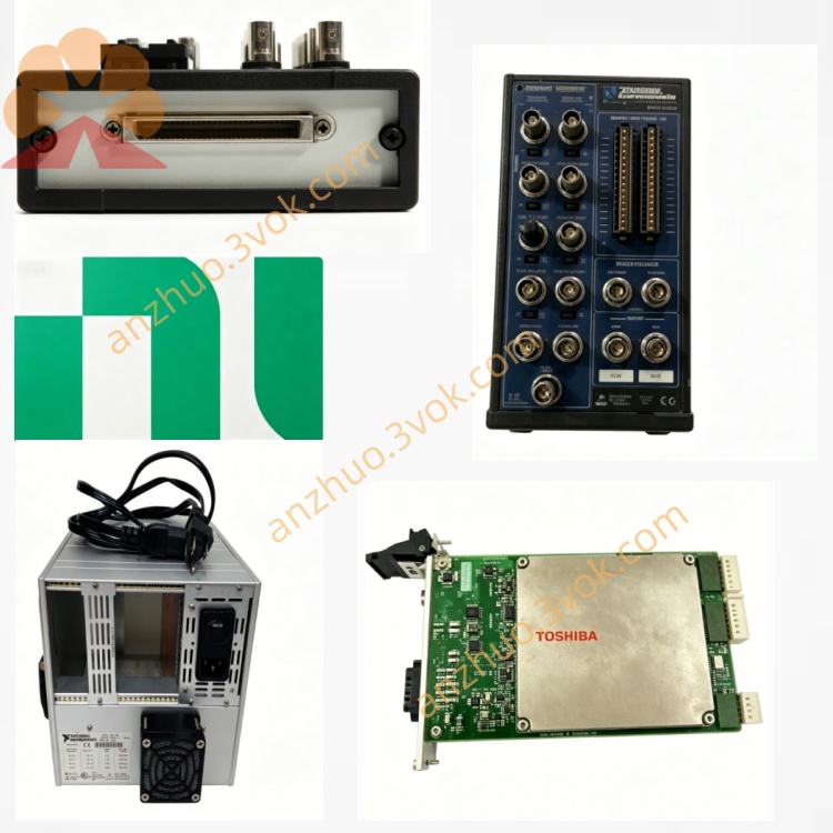
NI PXI‑5154 1GHz 2GS/s 8‑Bit PXI Oscilloscope
Description
Model Explanation
PXI: 3U standard PXI hybrid bus, single slot, compatible with PXI/PXIe chassis and NI.
5154: NI 5100 series, representing 2 channels, 1 GHz bandwidth, 2 GS/s, 8-bit high-speed PXI oscilloscope NI.
Component Number (by memory):
780320‑01: 8 MB / channel
780320‑02: 64 MB / channel
780320‑03: 256 MB / channel
Technical Specifications (25℃, preheating 15 min):
Channels: 2 analog inputs, synchronous sampling NI.
Resolution: 8 bits.
Sampling Rate: Real-time: single channel 2 GS/s, dual channel 1 GS/s; equivalent time: 20 GS/s (repeated signal).
Analog Bandwidth: 1 GHz (‑3 dB), DC–1 GHz, VSWR < 1.27 NI.
Input Voltage Range: 0.1/0.2/0.5/1/2/5 Vpp (±50 mV to ±2.5 V) NI.
Input Impedance: 50 Ω ±2% (fixed, not selectable 1 MΩ) NI.
Coupling Mode: AC / DC / GND (per channel independent) NI.
Onboard Memory: 8/64/256 MB / channel.
Rise Time: ≤350 ps (50 Ω, 10%–90%) NI.
Trigger: edge, window, hysteresis, digital, immediate, software; 5 ps time resolution; pre / post trigger.
Clock: internal 2 GHz VCSO; external 10–200 MHz; phase-locked PXI 10 MHz reference.
Power Consumption: approximately 24 W NI.
Size / Weight: 3U single slot, approximately 480 g.
Environment: operating 0–55℃; storage –40–70℃; humidity 10%–90% RH (no condensation).
Signal-to-Noise Ratio SINAD: typical 40 dB (ENOB ≈ 6.5 bits).
Crosstalk: 100 MHz <‑65 dB; 1 GHz <‑40 dB.
Interface and Communication Configuration
Front panel interface NI
2×BNC (CH0/CH1): analog input (50 Ω)
1×BNC (TRIG): external analog trigger input
1×SMB (CLK IN): external sampling clock / reference
1×SMB (CLK OUT): internal clock / reference output
2×SMB (PFI0/PFI1): digital trigger I/O, programmable function interface Indicator light
PWR (Green): Power supply is normal
RUN (Green): The acquisition is constantly on, waiting for trigger to flash
ERR (Red): Overheating, overcurrent, PLL lost lock, configuration error
Bus and Synchronization NI
PXI mixed bus, supports trigger bus, Star trigger, RTSI
Multi-module synchronous phase error < 50 ps, scalable to 34-channel coherent acquisition
Software driver NI
NI-SCOPE driver, supports LabVIEW, TestStand, Python, C#
NI MAX: Device management, self-check, configuration, calibration
Soft front panel SFP, high-speed waveform analysis, streaming inventory support Core function
1 GHz ultra-high bandwidth + 2 GS/s sampling: Covers RF, microwave, and high-speed digital signals, capturing sub-350 ps edges.
Equivalent 20 GS/s sampling: Ultra-high time resolution for repetitive signals, precise measurement of jitter, timing, and eye diagrams.
Maximum 256 MB/channel deep storage: Long-term high-speed recording, multi-segment waveform acquisition, long-term streaming.
50 Ω fixed impedance + AC/DC/GND coupling: Optimal matching for high-frequency signals, suitable for RF/microwave testing NI.
5 ps precise trigger and time base: Multiple trigger modes, precise capture of transient events and pulse signals.
High-speed streaming acquisition: Continuous data transmission and storage, suitable for long-term monitoring and mass production testing NI.
Multi-module ps-level synchronization: Star trigger / RTSI extends multi-channel coherent system, meeting MIMO radar/communication testing NI. Applicable scenarios
RF and microwave testing: RF / modulation / pulse signals within 1 GHz, radar, satellite communication, time-domain / frequency-domain analysis, NI.
High-speed digital testing: ultra-high-speed interfaces, FPGA, clock / jitter, eye diagram testing (edge < 400 ps), NI.
Semiconductor testing: high-frequency transient, pulse, RF parameters, high-speed acquisition of process characteristics, NI.
Radar and electronic warfare: pulse radar, signal intelligence, capture of high-speed transient electromagnetic signals, NI.
Research and defense: pulse laser, high-speed physics, transient electromagnetic, mass spectrometry, particle physics experiments, NI.
High-speed automated testing: high-speed boards for consumer electronics, aerospace, life sciences, and mass production testing, NI.
User and maintenance instructions
Installation and power-on
Power off for installation, single slot fixed; chassis reliably grounded to prevent static electricity NI.
Power on for 15 minutes for preheating, NI MAX self-check without hardware errors NI.
Keep ventilation during operation, temperature ≤ 55℃, do not block fans NI.
Connections and operations
High-frequency / RF signals use 50 Ω high-precision coaxial cables, BNC tightened to reduce reflection and loss NI.
Input prohibited > ±3 V (5 Vpp range), to avoid damaging the front end NI.
Trigger source preferentially selects signals within the channel, set appropriate trigger level to avoid false triggering; high-speed signals prefer edge triggering.
Multiple modules synchronize using PXI Star trigger to ensure ps-level phase consistency NI.
Maintenance and calibration
It is recommended to conduct NIST traceable calibration once every 2 years; daily internal self-calibration to compensate for temperature drift and time base errors.
Regularly clean BNC/SMB interfaces of dust, keep dry; for long-term idle, add a dust cap NI.
Environment free of condensation, humidity 10%–90% RH, away from strong electromagnetic interference and vibration NI.
Do not plug in or out cables while powered on; avoid severe vibration and impact NI.
Get a Quote