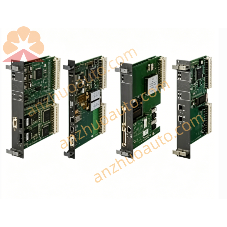
GE IS200SCTLG1ABA Mark VI Current Transformer Signal Interface Board
Description
GE IS200SCTLG1ABA Contact Input Terminal Board
Product Documentation - Condensed Edition
Product Identification and Overview
The IS200SCTLG1ABA is a simplex contact input terminal board engineered for the GE Innovation Series drive control system. It functions as the primary interface for sensing up to 24 external dry contact inputs and converting their states into digital data for the drive's core processing unit. The assembly consists of a base printed circuit board and a mezzanine-mounted Voltage-Controlled Oscillator (VCO) communication card. The "L" suffix in the part number signifies specific regulatory compliance, while "1A" indicates the functional revision level. This board is typically deployed in a single, non-redundant configuration within the drive's main control cabinet.
Core Functionality
The fundamental purpose of the IS200SCTLG1ABA is to provide a galvanically isolated, noise-immune pathway for the drive control system to monitor the open or closed status of external switches, relay contacts, and discrete sensors. The board accomplishes this by supplying a 24 VDC wetting voltage to each input loop. When an external contact closes, current flows through an optical isolator on the board. The scanning logic on the board multiplexes the status of all 24 optocouplers into a serial digital stream. The VCO mezzanine card converts this stream into a frequency-modulated signal for transmission to the DSP processor rack, typically over a fiber-optic or coaxial link. This frequency-domain transmission is the hallmark of the Innovation Series I/O architecture, providing exceptional common-mode noise rejection.
Hardware Architecture and Component Layout
The IS200SCTLG1ABA is built on a multi-layer PCB conforming to the 6U Eurocard form factor. Its physical construction is ruggedized for the thermal and vibrational environment of an industrial drive cabinet.
Input Channel Array
The board hosts 24 identical, independently isolated contact input channels. Each channel's circuitry consists of a two-position terminal block connection, a series current-limiting resistor, and a high-speed optical coupler. The components are arranged in three distinct banks of eight channels each, with their corresponding terminal block headers aligned along the vertical axis of the board. The dense layout is achieved while maintaining adequate creepage and clearance distances for the isolation voltage ratings.
Logic and Scanning Core
At the center of the board, a Complex Programmable Logic Device (CPLD) or a dedicated Application-Specific Integrated Circuit (ASIC) performs the critical scanning and data marshaling functions. This device runs a continuous loop, sequentially enabling each of the 24 optocoupler output buffers and capturing the resulting logic state. The captured 24-bit parallel word is serialized and shifted out to the VCO interface connectors. The scan rate is deterministic, providing a full input refresh every few hundred microseconds.
Mezzanine VCO Interface
The board is designed as a carrier for a VCO mezzanine card. A pair of high-density, surface-mount stacking connectors (designated J1 and J2) is positioned for vertical mounting of the daughtercard. These connectors carry the power supply rails, the serialized contact status data, and control signals between the base board and the VCO card. The mechanical design ensures a rigid connection without additional bracketing.
Front Panel and Connectors
A full-height aluminum front panel is attached to the PCB assembly. It serves dual purposes: a structural stiffener and the physical interface for all field wiring. Captive screws at the top and bottom secure the board into the card rack guide rails. The panel provides access to the three pluggable terminal strip sections for the 24 contact inputs and a separate connector for the wetting voltage source. A cutout is provided for the VCO card's BNC or ST-style fiber optic transmitter connector.
Connector Pinout and Signal Definitions
Terminal Strips for Contact Inputs (TB1, TB2, TB3)
These are three separate, eight-position pluggable terminal blocks. Each individual channel occupies two adjacent terminals. Terminal 'A' of each pair is the signal input and is connected internally to one side of the optical isolator's LED through the current-limiting resistor. Terminal 'B' is the 24 VDC common return path. The terminals are rising-cage clamp type, accepting 0.5 to 2.5 square millimeter conductors.
Signal mapping is sequential. TB1 handles inputs 1 through 8. TB2 handles inputs 9 through 16. TB3 handles inputs 17 through 24. The terminal blocks are mechanically keyed with unique pinning to prevent cross-insertion during maintenance.
Wetting Voltage Input (TB4)
This is a smaller, four-position pluggable terminal block. Two positions are dedicated for the +24 VDC wetting voltage supply input, and two for its return. This allows the board to be powered from an external isolated bulk supply or daisy-chained from an adjacent board's wetting voltage bus. An on-board fuse protects the 24V distribution.
Mezzanine Connectors (J1, J2)
These connectors are not field-serviceable. They provide the electrical link between the base board and the VCO card. J1 predominantly carries power and control signals. J2 carries the high-speed serial data stream. The pin assignment is specific to the family of compatible VCO cards.
Backplane Connector (P1)
A 96-pin DIN 41612 male connector is soldered to the rear edge of the PCB. It mates with the system's passive control backplane. Power pins deliver regulated +5 VDC for logic and +24 VDC for the onboard wetting bus option. Specific pins are also allocated for rack address encoding, allowing the board to identify its physical slot location to the software configuration tool.
Detailed Specifications
Input Section
Number of Channels: 24, non-isolated from each other within a bank, but bank-isolated from logic.
Input Type: Dry contact sensing only. Applying external voltage will damage the board.
Internal Wetting Supply: 24 VDC nominal, 21.6 to 26.4 VDC operational range.
Current per Closed Contact: 10 mA nominal at 24 VDC.
Input to Logic Isolation: 500 VDC continuous, optical.
Debounce Filter: Fixed hardware filter, 2 milliseconds typical activation time. State changes faster than this are rejected.
Contact OFF State Voltage: 24 VDC is present across an open contact.
Contact ON State Voltage: Approximately 0 VDC (closed contact shorting the terminals).
Power Supply Section
Logic Supply: +5 VDC ±5%, sourced from P1 backplane. Maximum current draw is 0.8 A (excluding VCO card).
Wetting Supply for Output: +24 VDC sourced either from P1 backplane or from TB4. The board's total wetting current capacity is fused at 0.5 A, providing sufficient margin for all 24 channels to be closed simultaneously (240 mA total).
VCO Card Power: Power for the VCO card is passed through the J1/J2 connectors from the base board's logic supply.
Mechanical
Form Factor: Standard 6U x 220 mm single-slot Eurocard.
Height: 233.35 mm.
Width: 30.48 mm (6T front panel).
Depth: 220 mm from front panel to rear of P1 connector.
Weight: 0.42 kg (base board only).
Terminal Wire Range: 20 to 14 AWG (0.5 to 2.5 mm²).
Environmental
Operating Temperature: 0 to 60 degrees Celsius at card rack inlet.
Storage Temperature: -40 to +85 degrees Celsius.
Relative Humidity: 5 to 95 percent, non-condensing.
Cooling: Forced air convection required. Minimum 200 LFM airflow across the board surface is assumed.
Scanning Performance
Scan Rate: 40 kHz nominal, resulting in a full 24-channel update every 25 microseconds.
VCO Modulation: Frequency Shift Keying (FSK). Mark (logic 1) and Space (logic 0) frequencies are specific to the VCO card model but are typically in the megahertz range.
System Latency: Total time from physical contact closure to DSP application variable update is less than 1 millisecond, including debounce filter, scan, serialization, transmission, and DSP read cycle.
Operational Theory
Signal Path from Field to Processor
The operational sequence begins in the field. A maintenance override switch, a pressure switch, or a relay auxiliary contact is wired across a channel's two terminals. When this external contact closes, it completes a circuit loop. Current flows from the internal 24 VDC wetting bus, through the current-limiting resistor, through the external closed contact, and through the LED internal to the optical coupler, returning to the 24V common. The LED emits light proportional to the current.
Optical Isolation and Debouncing
The light from the LED falls on a phototransistor across a transparent dielectric gap. The phototransistor saturates, effectively connecting its output to the logic common. This transition is captured by a Schmitt trigger buffer on the logic side, which squares up the signal edge and provides the initial debounce filtering. The buffer's output is routed to the scan logic's parallel input register. The galvanic isolation is physically realized in the micron-scale gap inside the optocoupler package, preventing any conductive path between the potentially harsh field wiring environment and the sensitive digital core.
Parallel-to-Serial Conversion
The scanning CPLD contains an address counter that runs continuously from 0 to 23. This counter drives a multiplexer that connects one of the 24 conditioned optocoupler outputs to a shift register's input. For each address, a clock pulse latches the single-bit state into the shift register. After 24 clock cycles, a complete snapshot of all inputs is held in the shift register. The CPLD then generates a framing pulse and shifts the entire 24-bit word out serially to the VCO card interface at a high clock rate, initiating the next scan cycle immediately.
Frequency Modulation and Link Transmission
The VCO card receives the serial NRZ data stream. A logic '1' commands the VCO to output a higher frequency carrier wave. A logic '0' commands a lower frequency. This FSK signal is amplified and drives either an LED transmitter for fiber optics or a line driver for coaxial cable. The signal propagates across the physical medium to the DSP rack.
DSP Register Update
In the DSP rack, a receiver card demodulates the FSK signal, recovering a clock and the serial data. A deserializer reconstructs the 24-bit parallel word. This word is then presented on the DSP's parallel peripheral bus at a specific memory-mapped address. The drive's application firmware reads this address on every control frame, making the 24 discrete input states available for logical operations, protection functions, and sequencing.
Integration and Configuration
Board Population and Installation
The IS200SCTLG1ABA must first be populated with a compatible VCO mezzanine card. The VCO card is aligned with the J1 and J2 connectors and pressed firmly into place. The assembled unit is then inserted into the designated slot in the control rack, ensuring the P1 backplane connector engages smoothly. The front panel captive screws are tightened to secure the board.
Field Wiring Connection
The three pluggable terminal blocks are removed from the board headers. Field wiring, consisting of twisted-pair cables for each channel, is terminated on the terminal blocks outside the rack for ease of assembly. One wire of the pair lands on the channel's signal terminal, and the other lands on the corresponding common return terminal. No shield termination is typically required for dry contact inputs, though a single-point shield ground for the cable bundle can be used if specified by system documentation. The wired terminal blocks are then re-inserted into their keyed headers.
Software Integration in ToolboxST
Within the GE ToolboxST engineering software, the hardware configuration tree for the drive must include the IS200SCTLG1ABA. The engineer inserts a module from the "Discrete I/O" library, selecting the exact catalog number. The software prompts for the rack number and slot number, which must match the physical location. Upon successful configuration, the software automatically generates a set of 24 Boolean variable tags. These tags, named by default CTL_IN_01 through CTL_IN_24, can be renamed by the application programmer to reflect the function of each connected device, such as "MCC_Breaker_Closed" or "Emergency_Stop_OK". The tag state is TRUE when the contact is closed and FALSE when the contact is open.
Technical Specifications Summary
Electrical ratings: 24 VDC nominal contact wetting voltage. Input current is limited to 10 milliamperes per channel. Logic power is 5 VDC at 0.8 amperes maximum.
Isolation ratings: 500 VDC continuous from input terminals to logic ground. Channel-to-channel operational voltage is 300 VDC maximum within the same terminal block.
Temporal performance: Hardware debounce time of 2 milliseconds. Scan period of 25 microseconds for all 24 channels. Total latency from contact closure to application logic variable update is guaranteed less than 1 millisecond.
Physical dimensions: 6U height, 6T width, 220 millimeter depth. Weight of 0.42 kilograms. Convection cooling required.
Connector types: Pluggable rising-cage clamp terminals for field I/O, 96-pin DIN 41612 for backplane, and proprietary stacking connectors for the VCO mezzanine card.
Part Number Nomenclature Decoding
The catalog string IS200SCTLG1ABA can be parsed as follows. "IS200" designates the Innovation Series 200 class of drive control components. "SCTG" is the functional designator for this specific simplex contact input terminal board family. "L" is the compliance designation, covering a specific set of international standards for safety and electromagnetic compatibility. "1A" specifies the major and minor hardware revision levels. "BA" is a manufacturing and artwork revision code. This complete string is essential for correct spare part ordering and software configuration matching.
Application Notes
The IS200SCTLG1ABA is optimally applied in scenarios requiring the monitoring of a moderate number of discrete, low-voltage contacts. Typical field devices include motor winding thermostat contacts, circuit breaker auxiliary status contacts, level switch outputs, and operator pushbutton or selector switch contacts. The internal 24 VDC wetting voltage is suitable for clean, dry contacts. For contacts exposed to corrosive atmospheres or with heavy oxidation, a higher wetting voltage or sealing current may be required, which is beyond the design scope of this board and would necessitate external interposing relays.
The board's simplex nature makes it suitable for non-safety-critical status monitoring. For drive protection functions requiring a voted, redundant architecture, a triple modular redundant (TMR) I/O system is required. The SCTG board cannot be used in such architectures. The 2-millisecond debounce filter is tuned for industrial relay and switch contacts. It is not suitable for high-speed pulse counting or the direct interface with solid-state proximity sensors without mechanical contact bounce.
Get a Quote