
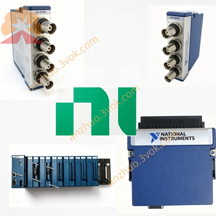
NI PXI-7811R Virtex-II Digital RIO FPGA Module
Description
II. Model Interpretation
PXI: 3U single slot, standard PXI bus, supports trigger/RTSI synchronization
7811: The first generation of R series digital RIO; 1=160 channels; 1= Basic FPGA scale
R: Reconfigurable I/O (reconfigurable I/O), onboard user-programmable FPGA
III. Technical Parameters (25℃)
1) FPGA Core
Model: Xilinx Virtex-II XC2V1000 (1 million gates)
Logic Resources: 10,240 flip-flops, 720 kbit block RAM, 40 18×18 multipliers
Clock: Maximum 200 MHz; I/O clock 40 MHz
Configuration: LabVIEW FPGA graphical programming, supports online reconfiguration
2) Digital I/O (DIO)
Channel Count: 160 bidirectional TTL channels, each channel independently configurable
Rate: Each channel up to 40 MHz; supports bilateral edge sampling
Function Modes: Input, Output, Counter/Timer, PWM, Encoder (A/B/Z), Custom Protocol
Electrical: TTL level (high ≥ 2.4 V, low ≤ 0.4 V); Maximum drive 24 mA per channel
Termination: Optional 50 Ω differential termination (for some channels)
3) Memory and Data Transfer
Onboard FIFO: 80 KB (40 KB each for input/output)
DMA: Supports PXI bus DMA, maximum 132 MB/s stream transfer
Trigger: PXI trigger bus (8 channels), RTSI bus, synchronization accuracy < 25 ns
4) Physical and Environmental
Form: 3U, single-slot PXI; size 160 mm × 100 mm
Connector: 4×68-pin VHDCI high-density female connector
Power Supply: +3.3 V (650 mA), +5 V (9 mA); power consumption approximately 2.2 W
Temperature: 0 ℃ ~ 55 ℃ (standard); optional -40 ℃ ~ 85 ℃ wide temperature version
Weight: Approximately 152 g
IV. Interface and Communication Configuration
1) Hardware Interface
I/O Connectors: 4×68-pin VHDCI, divided into 4 groups (each group 40 channels), with shielding
Backplane Bus:
PXI Local Bus: Data/Control Transmission
PXI Trigger Bus: Multi-module synchronization (25 ns accuracy)
RTSI: Cross-card / Cross-rack synchronization, supports 8 trigger + 1 clock
Clock: Internal 40 MHz crystal oscillator; supports external clock input (10–40 MHz)
2) Software and Drivers
Driver: NI-RIO, compatible with LabVIEW, LabVIEW FPGA, LabVIEW Real-Time
Development Process:
LabVIEW FPGA write hardware logic (graphical)
Compile and download to onboard FPGA
Host / Real-time system communicates with FPGA through DMA / registers
Supported Functions: Custom timing, hardware closed-loop, protocol parsing, pulse generation, event counting
V. Core Functions
160-channel high-speed configurable DIO, 40 MHz parallel processing
Each channel independent direction / mode, supports synchronous pulses, high-speed sampling, encoder feedback, PWM output, suitable for high-density digital quantity control.
User-defined FPGA hardware logic, 25 ns hard real-time Without the need for an external controller, the onboard FPGA directly performs closed-loop, timing, and decision-making, without the delay of an operating system, making it suitable for ultra-high-speed control.
Rich counters/timers and protocol support
Built-in 32-bit counter (up to 40 MHz), PWM generator, quadrature encoder interface; customizable SPI, I2C, UART, parallel bus, etc. protocols.
Precise synchronization of multiple modules (<25 ns)
Support for PXI trigger/RTSI bus, multi-card/multi-box synchronization, enabling the construction of large-scale parallel test systems.
High-bandwidth DMA data streaming transmission
80 KB FIFO + DMA, enabling 40 MHz continuous sampling/waveform generation, suitable for high-speed data recording and playback.
Six, Application Scenarios
High-speed digital testing and measurement
Semiconductor chip testing, functional verification of digital circuit boards, high-speed pulse generation/collecting, alternative to logic analyzers.
Hardware-in-the-Loop (HIL) real-time simulation
Motor control HIL, power electronics simulation, robot controller testing, requiring microsecond-level closed-loop scenarios.
Industrial automation and motion control
High-speed sorting/packaging lines, multi-axis synchronous motion (encoders + pulse instructions), custom PLC substitution, high-speed I/O interlock systems.
Customized communication protocols and interfaces
Military/aerospace-specific protocols, interface conversion for old equipment, high-speed parallel bus simulation, sensor signal conditioning.
Large-scale parallel data acquisition
Multi-channel sensor array (digital output type), high-speed sampling of vibration/impact, distributed test system synchronization.
Seven, Usage and Maintenance Instructions
1) Installation and Power On
Insert the PXI into any slot, tighten the fixing screws, and ensure the chassis is reliably grounded. Before powering on, check that the 4 68-pin VHDCI cables have no short circuits or loose connections to avoid damage to FPGA I/O.
Allow the machine to preheat for 15 minutes before performing precise tests to ensure stable timing.
2) Wiring and Configuration
Cables: Use shielded VHDCI cables. Separate digital signals from analog/power lines to reduce crosstalk; single-ended cable length ≤ 3 m, differential ≤ 10 m.
Configuration: Confirm the hardware through NI MAX; when compiling logic in LabVIEW FPGA, clock constraints ≤ 40 MHz to avoid timing violations.
Debugging: Run basic I/O tests without load first to confirm the channels are normal before connecting the load; use FPGA probes to monitor hardware signals in real time.
3) Daily Maintenance
Regularly clean the VHDCI connectors, check the integrity of the shielding layer, install dust caps for long-term inactivity to prevent oxidation and dust accumulation.
Calibration: Once a year, use the NI digital I/O calibration tool to verify channel levels, timing, and trigger accuracy.
Firmware: Regularly update NI-RIO drivers and FPGA firmware to fix compatibility issues and optimize timing performance.
Get a Quote