
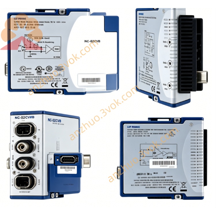
NI PXI-6651 PXI Timing & Synchronization Module
Description
II. Model Interpretation
PXI: Standard 3U single-slot structure, compatible with both PXI and PXIe hybrid slots, suitable for adapting to PXI backplane clocks, triggers, and star-shaped trigger buses.
6651: Belongs to the 665x series of precise timing synchronization products. The last digit represents the product's function positioning. 1 indicates a synchronous slave model, without onboard high-precision clock, only responsible for signal reception, forwarding, and routing.
Product Positioning: As a synchronous expansion unit, used in conjunction with the main clock module to expand the system's synchronization capacity.
III. Technical Parameters (25℃ Normal Temperature)
1. Clock Signal Parameters
External clock input frequency range: 1 MHz ~ 105 MHz, supports both sine wave and square wave signal forms
Input interface impedance: 50 Ω
Supported signals: Can receive and forward the standard 10 MHz backplane reference clock PXI_CLK10 of the chassis
2. Trigger and Synchronization Parameters
Programmable Function Interface: 2 channels of PFI, configurable as signal input or output
Backplane Bus Support: Complete control of 8 channels of PXI general trigger bus and PXI star-shaped trigger bus
System Synchronization Precision: Synchronization deviation of multiple modules and multiple chassis is less than 5 ns
3. Physical and Environmental Parameters
Form Specification: 3U single-slot
Status Indicators: 2 sets of three-color LED indicators, respectively indicating power supply, signal lock, and operating status
Operating Temperature: 0 ℃ ~ 55 ℃
Electrical Characteristics: Compliant with PXI specifications, with basic signal anti-interference capabilities
IV. Interface and Communication Configuration
1. Hardware Interfaces
Front Panel Interfaces: A total of 3 SMB interfaces, respectively for external clock input CLKIN, PFI0, PFI1
Backplane Bus: Connected to the PXI standard bus, linking the 10 MHz reference clock of the chassis, 8 channels of trigger buses, and star-shaped trigger buses, achieving signal intercommunication between board cards.
2. Software and Drivers
Companion Driver: NI-SYNC, providing signal configuration, routing, and synchronization management functions for the module.
Development Environment: Supports mainstream development platforms such as LabVIEW, C/C++, Python, and TestStand, enabling synchronous logic programming and status monitoring.
V. Core Functions
External Clock Reception and Distribution
Can connect to external high-frequency clocks or standard 10 MHz reference clocks, forwarding the signals to the local PXI backplane, providing a unified time reference for all board cards in the chassis.
Flexible Signal Routing
Supports freely mapping the front panel CLKIN and PFI signals to the PXI trigger buses, star-shaped trigger buses, or can also lead the backplane signals to external devices to build diverse synchronization topologies.
Nanosecond-level Multi-Device Synchronization
Relying on star-shaped triggers and dedicated synchronization circuits, combined with the main clock module, achieving high-precision timing alignment between single-chassis multiple boards and multiple chassis.
Expansion of the Synchronization System
As a slave module expansion of the synchronization node, without adding expensive main clock modules, expand the system's synchronization channels and coverage, optimizing the overall cost.
VI. Application Scenarios
Large-scale PXI Automated Test System
Multi-board card, multi-chassis ATE equipment, unified clock and trigger signals, ensuring consistent timing for collection and output actions.
Radio Frequency and Microwave Testing
Allocate a 10 MHz standard reference clock to achieve synchronization of signal sources, spectrum analyzers, receivers, etc., of radio frequency instruments.
High-speed Data Acquisition System
Multiple digital instruments and high-speed I/O cards are linked for testing, eliminating timing deviations, ensuring synchronous data acquisition.
Distributed Industrial Measurement and Control
Collaborative work of multiple sites, multiple chassis industrial control equipment, achieving unified timing and collection sequences between remote sites.
Semiconductor Chip Testing Complex timing verification scenarios provide synchronous triggering and clock reference for multiple sets of test units.
VII. Installation and Maintenance Instructions
1. Installation and Power On
Insert the module into the PXI chassis slot when the power is off, tighten the fixing screws to ensure reliable grounding of the chassis. After powering on, the driver will automatically complete the hardware self-check, and observe the panel LEDs to confirm that the module has been powered on normally. During equipment operation, keep the chassis ventilated to avoid temperature accumulation affecting signal stability.
2. Wiring and Operation
The interface uses 50 Ω standard SMB shielded cables for connection. For high-frequency clock signals with a frequency greater than 10 MHz, try to shorten the cable length and ensure that the lengths of each branch cable are consistent to reduce timing offset. This module cannot be used independently as the system master clock. It must be used in combination with PXI-6652, PXI-6653 and other master clock modules or external reference clocks. According to the test requirements, configure signal routing and PFI input/output directions in the software.
3. Daily Maintenance
Regularly wipe the dust on the SMB interface surface, check if the cable connections are loose, and avoid poor contact causing abnormal signals. When the module is idle for a long time, install a dust cap on the interface. The module is a pure digital signal circuit and does not require regular calibration. Regularly update the NI-SYNC driver and firmware to ensure stable functionality and compatibility.
Get a Quote