
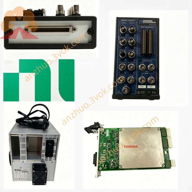
NI PXI-6561 LVDS Digital Waveform Instrument
Description
II. Model Interpretation
PXI: 3U single-slot PXI module, compatible with PXI/PXIe mixed slots.
6561: 656x (LVDS high-speed differential waveform instrument); 1 = 100 MHz (6562 = 200 MHz).
Core Identifier: 16-channel LVDS differential, 100 MHz, DDR 200 Mb/s, SMC synchronous core, onboard deep memory, low noise anti-interference.
III. Technical Parameters (25℃) General
Channel: 16 LVDS differential bidirectional I/O (each channel has independent direction in SDR mode).
Level: LVDS standard differential (approximately ±350 mV), compatible with high-speed differential interface.
Drive: Differential drive, strong anti-common-mode interference, suitable for long-distance / strong-noise environments.
Memory: 2/16/128 Mbit / channel (depending on model), supports ultra-long differential waveform sequences.
Rate and Timing
Clock: Maximum 100 MHz (internal / external / reference clock), range 48 Hz to 100 MHz.
Data Rate: SDR = 100 Mb/s, DDR = 200 Mb/s (dual-edge sampling).
Edges: Rising / Falling / Delayed edges selectable, channel skew ±500 ps (typical).
Trigger: PXI trigger bus, STAR trigger, 4-channel PFI, minimum pulse width 20 ns.
Synchronization: SMC (Synchronous with Storage Core), multi-module nanosecond-level synchronization.
Jitter: Typical 15 ps rms (cycle), meets high-speed differential timing requirements.
Physics and Environment
Size: 3U single slot (160×100 mm).
Power Consumption: Typical 12 W, maximum 18 W.
Connectors: 12-channel InfiniBand (LVDS I/O) + 3×SMB (clock / trigger).
Temperature: 0 to 55°C (commercial); extended grade -40°C to +85°C.
IV. Interface and Communication Configuration
Hardware Interface
I/O: 12-channel InfiniBand connector, recommended cable adapted to LVDS differential signal.
Clock / Trigger: 3×SMB (CLK IN/OUT, PFI), supports external 100 MHz clock input.
Bus: PXI bus, DMA bus master mode, low CPU usage.
Software and Drivers
Driver: NI-HSDIO, paired with Digital Waveform Editor waveform editing software.
Development Environment: LabVIEW, Python, C#, TestStand, supports scripted sequences, PRBS generation.
Synchronization: PXI trigger / RTSI/STAR, mixed-signal synchronization with digitizers, AWGs, etc.
V. Core Functions
16-channel LVDS differential high-speed bidirectional I/O: standard LVDS level, strong anti-interference, low power consumption, high rate; each channel has independent direction in SDR mode, flexible configuration of differential bus / control signals.
100 MHz clock + 200 Mb/s DDR: generate / capture high-speed differential digital timing, protocol signals (such as LVDS, HDMI, PCIe, Ethernet physical layer); ±500 ps skew, meets high-speed differential timing verification requirements.
Deep memory + advanced sequences: each channel up to 128 Mbit, stores ultra-long differential waveforms; supports looping, branching, conditional triggering, PRBS, simulating complex differential communication workflows.
SMC synchronous core: multi-module synchronization expanded to hundreds of channels, nanosecond-level timing alignment; seamless integration with digitizers, AWGs, power supplies, building a complete mixed-signal ATE.
Low noise and high stability: LVDS differential design suppresses common-mode noise, suitable for industrial strong interference, long-distance transmission scenarios; programmable input filtering, further improves signal integrity.
VI. Application Scenarios LVDS Interface Chip Verification: Timing/functional tests, protocol simulation, signal integrity verification for LVDS transceivers, buffers, and HDMI/DisplayPort interface chips.
High-speed Communication and Network Devices: Differential signal tests for Ethernet PHY, PCIe, USB3, optical communication modules, timing compliance verification, bit error rate testing.
FPGA/SOC High-Speed Interface Testing: LVDS high-speed buses, parallel interfaces, clock synchronization tests for FPGA/CPLD, MCU, and SoC.
Industrial Control and Automotive Electronics: High-speed differential I/O tests for vehicle ADAS, autonomous driving modules, industrial PLCs, long-distance communication verification, strong interference environment testing.
Mixed-Signal ATE/FCT: PCB functional tests, simulation of high-speed differential digital interfaces, acquisition/generation of control signals, synchronous analog measurement (voltage/current).
VII. Installation and Maintenance Instructions
Installation and Power On
Installation: Disconnect power, insert into the 3U slot of the PXI chassis, ensure reliable grounding of the chassis, and perform anti-static operation.
Power On: NI-HSDIO automatically self-checks after startup, no preheating required; avoid frequent cold-hot restarts.
Environment: Keep the air ducts unobstructed, 0-55℃; away from strong electromagnetic interference (motors, frequency converters).
Connection and Operation
Connection: Avoid frequent plugging and unplugging of InfiniBand interfaces, use dedicated LVDS shielded cables; ensure equal length and impedance matching for long-distance transmission.
Level Configuration: Confirm that the DUT is in LVDS standard level, avoid mixing with single-ended TTL/CMOS, to prevent damage to the device.
High-Speed Design: Strictly match impedance for 100 MHz differential signals, short traces, complete ground plane, reduce reflection and crosstalk.
Daily Maintenance
Interfaces: Regularly clean InfiniBand/SMB interfaces, prevent dust and moisture; install dust covers when idle.
Software: Update NI-HSDIO drivers and firmware to obtain function optimization and bug fixes.
Calibration: Digital circuits do not require regular calibration; check wiring tightness and cable integrity annually.
Get a Quote