
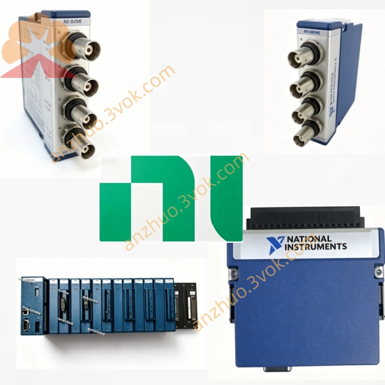
NI PXI‑2594 2.5 GHz 50‑Ohm Single SP4T Unterminated RF Multiplexer Module
Description
II. Model Interpretation
PXI: Standard PXI bus, compatible with PXIe mixed slots.
2594: NI high-frequency RF multiplexer series code, representing a 4-channel 2.5 GHz 50Ω RF multiplexer.
Full name: PXI-2594 4-channel 2.5 GHz 50Ω PXI RF multiplexer module.
Topology: Fixed 4×1 non-terminated multiplexer (4 input channels → 1 common output channel) NI.
III. Technical Parameters
(1) RF Core Characteristics
Frequency range: DC ~ 2.5 GHz (–3 dB).
Characteristic impedance: 50 Ω (full channel matching).
Insertion loss: Typical < 1.0 dB; Maximum < 1.35 dB (2.5 GHz).
Channel isolation: Typical ≥ 70 dB (1 GHz); ≥ 60 dB (2.5 GHz).
Voltage Standing Wave Ratio (VSWR): Typical ≤ 1.3:1; Maximum ≤ 1.5:1.
Maximum RF power: 10 W (40 dBm) / channel (continuous).
Maximum switching voltage: 30 Vrms / 30 VDC; Channel-to-ground isolation 30 V.
Maximum switching current: 500 mA (resistive).
(2) Switch and Relay Parameters
Relay type: Electromechanical RF relay, gold contacts, low contact resistance.
Channel configuration: 4 RF channels (CH0~CH3) + 1 common terminal (COM) NI.
Action time: Typical 6 ms, maximum 10.4 ms.
Mechanical life: 5×10⁷ times on-off (1 V/10 mA).
Electrical life: 1×10⁶ times (10 W/1 GHz).
Termination method: Default non-terminated; supports external 50Ω SMA terminator.
(3) Scanning and Triggering
Scanning list: Maximum 32,000 programmable scanning sequences.
Full-channel scanning rate: Maximum 150 times/second.
Trigger channel: Supports PXI backplane Trigger 0~Trigger 7 hardware trigger bus.
Minimum trigger pulse width: 150 ns (disable digital filtering).
(4) Physical and Environmental Parameters
Form specification: Standard 3U PXI single-slot module, compatible with PXIe mixed slots.
Front-end connector: 5 SMA RF connectors (4 channels + 1 common terminal).
Form size: 216 mm × 20 mm × 130 mm.
Weight: Approximately 0.29 kg.
Power supply: PXI backplane 3.3 V/5 V; Typical power consumption 0.8 W (3.3 V) + 2.5 W (5 V).
Operating temperature: 0 ℃ ~ 55 ℃.
Storage temperature: –20 ℃ ~ 70 ℃.
Relative humidity: 5% ~ 85%, no condensation.
IV. Interface and Topology Configuration
Front-end I/O interface (SMA)
4×1 mode (fixed): 4 independent RF channels (CH0~CH3) → 1 common terminal (COM); only 1 channel is connected to COM at the same time.
Connection example: Signal source → any of CH0~CH3 → COM → device under test (DUT).
Bus and software communication
Bus interface: Standard PXI backplane, compatible with PXIe mixed slots, automatically acquires power, clock, trigger.
Driver: Standard NI-SWITCH, compliant with IVI specification. Software support: LabVIEW, TestStand, LabWindows/CVI, Python, etc.
Basic functions: Hardware recognition, channel status reading, scan editing, trigger configuration, life count query.
Synchronization capability: PXI trigger bus enables high-precision synchronous switching of multiple modules.
VII. Core functions
2.5 GHz ultra-wideband switching: Covers DC to 2.5 GHz, suitable for 5G, WiFi, high-speed digital, etc. high-frequency signal routing.
50Ω precise impedance matching: Full-link 50Ω design, VSWR ≤ 1.3, minimizing reflection and loss.
Low insertion loss high isolation: 1.0 dB insertion loss + 70 dB isolation, ensuring high-frequency signal integrity.
Fixed 4×1 multiplexing: Simple topology, suitable for high-frequency switching scenarios with single input and multiple outputs or multiple inputs and single output in NI.
10 W high power carrying capacity: 10 W continuous RF power per channel, meeting medium-power RF testing requirements.
Relay life monitoring: Board-mounted counter records on/off times, supporting predictive maintenance.
SMA interface high reliability: Standard SMA connector, stable connection, suitable for high-frequency test cables.
VI. Applicable scenarios
RF communication testing: 5G/4G RF modules, WiFi/BT devices, antenna multi-path switching, signal routing.
Semiconductor testing: RF IC, high-speed digital chips, clock distribution, ATE high-frequency testing system.
High-speed digital testing: DDR, PCIe, USB4, etc. high-speed signal channel switching and verification.
General high-frequency testing: Multi-channel switching of signals within 2.5 GHz source, oscilloscope, spectrum analyzer.
RF aging testing: Long-term stability testing of medium-power RF components, multi-channel parallel aging.
VIII. Usage and Maintenance Instructions
Usage points
Installation: Insert into the 3U standard slot, lock the panel screws, keep away from strong electromagnetic interference; PXIe chassis prefer mixed slots.
Connection: Use 50Ω SMA RF cables, ensure the connectors are tightened, avoid loosening causing VSWR deterioration; minimize the length of the high-frequency signal path.
Electrical limits: Strictly follow the 30 V/10 W rated parameters; avoid electrostatic discharge (ESD), ground before operation.
Topology restrictions: Fixed 4×1, cannot be configured as other topologies; multiple groups of switching require multi-module cascading in NI.
Heat dissipation: Ensure good ventilation of the chassis, avoid overheating during 2.5 GHz high-power operation.
Maintenance instructions
Regular inspection: Inspect SMA connectors every quarter, clean dust, check for loose oxidation, focus on checking contact resistance of high-frequency connectors.
Life management: Regularly read on/off times, plan for relay replacement when approaching electrical life limit.
Environmental control: Maintain dry and ventilated conditions, temperature 0~55 ℃, avoid condensation and dust accumulation.
Fault handling: Check wiring, grounding and VSWR first for channel abnormalities; single-channel faults can be replaced with relays on-site.
Storage requirements: Disconnect cables when not in use, protect interfaces from dust, store in a dry environment of -20~70 ℃.
Calibration: Suggest annual calibration, test insertion loss, isolation, VSWR and channel consistency.
Get a Quote