
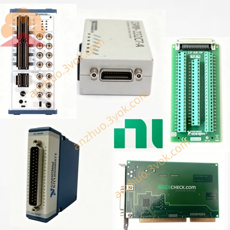
NI PXI‑2536 544‑Crosspoint FET Matrix Switch Module
Description
Model Explanation
PXI: PXI bus platform (modular instrument standard)
2536: Product serial number, representing 544 cross-point FET high-density matrix switch
Alias: NI-2536, PXI-2536 (FET 8×68 matrix)
Function Positioning: 8×68 single-line high-density matrix, FET without contact, ultra-high-speed, long-life signal routing NI
Technical Parameters
Cross-point Number: 544 (fixed 8 rows × 68 columns single-line matrix) NI
Relay Type: Field Effect Transistor (FET), no mechanical lifespan limit NI
Maximum Switching Voltage: ±12 VDC / 8 VACrms
Maximum Switching Current: 100 mA / channel
Maximum Switching Power: 1.2 W (single channel)
Bandwidth (–3 dB, 50 Ω): Typical 1 MHz
Thermal Emissivity: Typical < 5 μV
Channel Isolation Resistance: Typical > 1 GΩ (DC)
Path Resistance: Typical < 5 Ω (row to column)
Switching Time: Typical < 20 μs NI
Scan Rate: 50,000 cross-points per second NI
Maximum Drive Capability: 544 FETs (fully closed)
Trigger Characteristics: PXI trigger line 0–7, minimum pulse width 70 ns; hardware synchronization
I/O Connectors: 4 68-pin VHDCI motherhead
Size: 3U PXI single slot (216 × 20 × 130 mm)
Weight: Approximately 250 g
Operating Temperature: 0–55 °C
Interface and Communication Configuration
PXI Bus Interface: Standard 3U PXI backplane connector, power supply, trigger, clock and communication
Front-end I/O Connectors: 4×68-pin VHDCI, high-density signal output
Terminal Block (optional): TB-2625, etc., supports screw terminals or ribbon cable connections
Control Communication: PXI bus, compatible with NI- SWITCH, MAX, LabVIEW, TestStand NI
Trigger Synchronization: Hardware trigger input/output, nanosecond-level synchronization, improves test throughput NI
Expansion Capability: Multi-module cascading, can be extended to larger matrix scale
Core Function
High-density 8×68 matrix: 544 cross-points, single-slot integration, saves chassis resources NI.
FET Contactless Technology: Infinite mechanical lifespan, 50,000 switching times per second ultra-high-speed switching, suitable for high-frequency mass production NI.
Low Thermal Emissivity and High Isolation: < 5 μV thermal offset, > 1 GΩ isolation, suitable for low-level precision measurement.
Overvoltage Fault Protection: Built-in FET protection circuit to prevent overvoltage damage, improves system stability.
Hardware Trigger and Deterministic Timing: Minimum trigger pulse width of 70 ns, precise synchronization of multiple instruments NI.
On-board Relay Counters: Real-time monitoring of switching times, predicts maintenance cycle NI. Applicable scenarios
Semiconductor testing: Wafer testing, chip parameter testing, aging screening, high-density high-frequency switching NI.
PCB / electronic manufacturing: Circuit board conduction test, functional verification, batch production test NI.
Precise low-level testing: Sensor signal acquisition, instrument calibration, low-voltage signal switching.
Automated test system (ATE): High-density, high-speed rate test scenarios, shorten test cycle NI.
Small and medium-sized signal routing: Multi-channel signal switching in laboratory / R&D environment, balancing density and cost.
User and maintenance instructions
Key usage points
Installation: Standard 3U PXI chassis single slot, lock the panel, ensure the backplane connector is reliably connected.
Configuration: Set channel mapping, trigger parameters and scan sequence through NI-SWITCH or MAX software NI.
Cabling: 4×68-pin VHDCI connect to TB-2625 terminal block; strictly follow the ±12 V/100 mA limit, avoid overload.
Operation monitoring: Use the onboard relay counting function to regularly read the switching times, evaluate the module status NI.
Environment: Working temperature 0–55 °C, avoid strong electromagnetic interference, dust and condensation; must be well grounded to prevent FET malfunction.
Maintenance instructions
Regular inspection: Check the connector tightness, whether the terminal block wiring is loose, and clean the surface dust every quarter.
Life management: FET has no mechanical lifespan, but need to monitor electrical stress to avoid long-term overpressure / overcurrent operation NI.
Fault diagnosis: When the channel is not working or the signal is abnormal, first check the wiring and grounding, then diagnose the FET status through software; avoid electrostatic damage to the module.
Storage: When not in use for a long time, power off and store in a dry, dust-proof environment, add a dust cap to the connector to prevent moisture and oxidation.
Get a Quote