
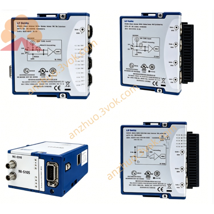
NI PXIe-5186-782058-02 8-channel High-Speed PXIe Oscilloscope Module
Description
I. Product Introduction
The NI PXIe-5186-782058-02 is a 2-channel, 8-bit, 5 GHz bandwidth, 12.5 GS/s sampling rate high-speed PXIe oscilloscope/digital instrument, belonging to the NI high-performance PXI Express instrument series. 782058-02 is the version with 1 GB large-capacity memory per channel, suitable for long-term, high-resolution, high-speed signal acquisition and analysis, widely used in RF, high-speed digital, transient signal testing scenarios.
II. Model Interpretation
NI: Brand logo of National Instruments.
PXIe: PXI Express, a high-speed modular instrument standard based on PCIe bus.
5186: Product serial number, representing 2-channel, 5 GHz bandwidth, 12.5 GS/s oscilloscope module.
782058: Basic component number.
-02: Suffix, indicating 1 GB on-board memory per channel (-01 is 32 MB / channel).
III. Technical Parameters
Number of channels: 2 synchronous sampling analog input channels.
ADC resolution: 8 bits.
Real-time sampling rate: Up to 12.5 GS/s (single channel).
Equivalent sampling rate (RIS): Up to 250 GS/s.
Analog bandwidth:
50 Ω path: DC–5 GHz.
1 MΩ path: DC–500 MHz.
Input impedance: Software selectable 50 Ω or 1 MΩ.
Input voltage range (peak-to-peak): 110 mV–10 V.
On-board memory: 1 GB / channel (782058-02).
Trigger type: Edge, pulse width, glitch, video, mode, sequence, external trigger, etc. NI.
Reference clock: Supports external 10 MHz/100 MHz input, internal low-jitter clock NI.
Physical specifications: Standard 3U PXIe module, size 16×10 cm, weight approximately 1.2 kg.
Environmental parameters: Operating temperature 0–55°C, storage - 40–70°C, humidity 10%–90% without condensation.
IV. Interface and Communication Configuration
Front panel analog input:
CH0/CH1: 50 Ω SMA and 1 MΩ BNC dual interface.
REF CLK/CLK IN: SMA, external reference clock input NI.
TRIG: SMA, external trigger input NI.
Bus interface: x4 PXIe Gen2, dedicated bandwidth 2 GB/s, supports DMA high-speed data flow NI.
Synchronous interface: Supports PXIe backplane trigger, star trigger, 10 MHz/100 MHz clock synchronization, synchronization accuracy < 10 ps between multiple chassis / modules.
Software interface: NI-DAQmx, NI-SCOPE driver, supports LabVIEW, C/C++, Python, etc. development.
V. Core Functions
Ultra-high-speed signal acquisition: 12.5 GS/s real-time sampling + 250 GS/s equivalent sampling, accurately capturing 5 GHz high-frequency and transient signals.
Flexible dual impedance adaptation: 50 Ω for RF/microwave, 1 MΩ for general electronic signals, software one-click switch.
Ultra-large depth storage: 1 GB / channel memory, supports long-term, high sampling rate continuous acquisition, reduces data segmentation.
Precise timing synchronization: Backplane clock and trigger bus, multi-box / multi-module synchronization accuracy < 10 ps, suitable for large-scale testing systems. Rich Triggering and Analysis: Multiple triggering modes, built-in FPGA real-time computing, supports FFT, eye diagrams, jitter analysis, etc.
Self-calibration and High Stability: Built-in precise reference, self-calibration to compensate temperature drift, ensuring measurement accuracy across the entire temperature range.
Six. Application Scenarios
Semiconductor Testing: Signal integrity, eye diagrams, jitter tests for high-speed digital chips, DDR, SerDes, RF ICs.
Aerospace and Defense: Radar pulses, satellite communication, electronic warfare signals, capture of high-speed transient events.
RF and Microwave: Frequency and time domain testing for 5G/6G, WiFi 7, millimeter wave components.
Automotive Electronics: Autonomous driving radar, high-speed buses, battery pulse signal acquisition.
Research and Laboratories: Frontier research such as ultrafast optics, plasma, material transient responses.
Seven. Usage and Maintenance Instructions Instruction Manual
Installation: Insert the PXIe chassis into any mixed slot while the power is off, and tighten the fixing screws; preferentially use shielded SMA/BNC cables (such as RG-223).
Wiring: RF signals use 50 Ω SMA, general signals use 1 MΩ BNC; external clock/trigger connect to the corresponding SMA port to ensure impedance matching.
Software configuration: Install the NI-SCOPE driver and PXI platform service, and identify the NI MAX module; set the sampling rate, bandwidth, impedance, trigger mode and memory depth; configure the clock source (internal/external) and synchronization routing.
Calibration: Preheat the system for 15 minutes upon startup; it is recommended to perform self-calibration and NIST traceability calibration once a year to ensure accuracy.
Maintenance instructions
Daily cleaning: Regularly wipe the front panel and connectors with a dry soft cloth to prevent dust from entering the interface; do not allow liquids to contact the module.
Connection check: Regularly check for looseness, oxidation or damage to the SMA/BNC connectors to prevent signal attenuation and impedance mismatch.
Environmental control: Working environment temperature 0–55°C, humidity < 90% without condensation, away from strong electromagnetic interference and vibration.
Fault troubleshooting: When there is signal abnormality, first check the cables and connectors; when synchronization fails, check the clock/trigger lines and backplane configuration; when data is lost, check the memory settings and bus bandwidth.
Long-term storage: Remove the module after power off, store it in a dry and cool environment to avoid static electricity and compression; storage temperature - 40–70°C.
Get a Quote