
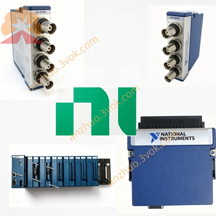
NI PXI‑2543 6.6GHz 50‑Ohm Solid‑State Dual SP4T RF Module
Description
II. Model Interpretation
PXI: PXI bus platform (old version); PXIe is PXI Express (replacement version)
2543: Product serial number, representing 6.6 GHz, dual 4×1, solid-state RF multiplexer
Alias: NI-2543, Dual 4x1 Terminated Mux, dual SP4T RF switches
Function positioning: 2 sets of independent 4-out-of-1 RF switches, solid-state, fully terminated, high isolation, parallel test expansion
III. Technical Parameters Basic parameters
Topology: 2 independent groups of 4×1 (SP4T) multiplexers, Bank A (CH0A to CH3A → COMA), Bank B (CH0B to CH3B → COMB) NI
Relay type: FET solid-state relay (without mechanical contacts)
Frequency range: DC to 6.6 GHz (–3 dB), minimum 10 MHz
Characteristic impedance: 50 Ω (nominal)
Terminal configuration: All channels and the common terminal are internally equipped with 50 Ω terminations
Electrical parameters
Maximum switching voltage: ±8 VDC
Insertion loss (typical): 1 GHz < 1.5 dB; 6.6 GHz < 6.1 dB
Isolation (typical): 1 GHz > 40 dB; 6.6 GHz > 30 dB
Switching time: typical 76 μs (trigger to stable)
Relay lifespan: infinite (solid-state), no mechanical wear
RF power: typical + 20 dBm (continuous)
Physical and environmental
I/O connector: RF 10×SMA female (8 channels + 2 common terminals); trigger 2×SMB (TRIG IN/OUT) NI
Size: 3U PXI single slot (approximately 100×160×20 mm)
Weight: approximately 300 g
Power consumption: 12 V ≈ 0.4 W; 3.3 V ≈ 1 W
Operating temperature: 0 to 55 °C
Storage temperature: –40 to 70 °C
IV. Interface and Communication Configuration
Front-end interface
RF interface: 10×SMA female
Bank A: CH0A, CH1A, CH2A, CH3A, COMA
Bank B: CH0B, CH1B, CH2B, CH3B, COMB
Trigger interface: 2×SMB
TRIG IN: external trigger input (150 ns pulse width)
TRIG OUT: trigger output, used for synchronizing other modules NI
Bus and control
Bus interface: standard 3U PXI backplane (PXI‑2543)/PXIe backplane (PXIe‑2543), power supply, trigger, clock, communication
Control software: compatible with NI‑SWITCH, MAX, LabVIEW, TestStand, Switch Executive
Driver support: NI‑DAQmx, NI‑VISA, providing VI and API function libraries
Trigger synchronization: PXI hardware trigger, nanosecond-level synchronization, supports multi-module cascading
Configuration method: software to set channel mapping, trigger parameters, scan sequence
Adaptation and expansion
Adaptation cable: SMA-SMA direct connection; optional SMA to BNC/SMB/MCX
Expansion capability: multi-module cascading, expand channel quantity, build large-scale RF switch system
V. Core Functions
Dual 4×1 independent switches: 2 groups of completely independent 4-out-of-1 routing, can simultaneously control two RF signals, support parallel testing, improve throughput NI.
DC to 6.6 GHz bandwidth: covers WiFi, Bluetooth, 2G/3G/4G, ISM frequency bands, etc., meets mainstream RF testing requirements.
Solid-state infinite lifespan: no mechanical contacts, suitable for 24/7 production scenarios, avoids mechanical fatigue, reduces maintenance costs.
All-channel 50 Ω terminations: all channels and common terminals are internally equipped with terminations, reduces signal reflection, improves measurement stability and repeatability.
High-speed switching + hardware trigger: μs-level switching speed, PXI hardware trigger synchronization, supports high-speed sequence scanning, adapted to automated test systems. High isolation and low loss: Ensuring signal integrity, reducing inter-channel interference, and improving test accuracy.
VI. Applicable Scenarios
Consumer electronics RF testing: WiFi, Bluetooth, NFC, GPS, 2G/3G/4G module function verification and mass production testing.
Semiconductor RF chip testing: Parameter testing, aging screening and function verification of RF ICs and mixed-signal ICs.
Multi-station parallel ATE testing: Dual 4×1 structure adapted to 2 parallel tests, improving test efficiency and reducing single-station costs (NI).
RF instrument expansion: Channel expansion of signal sources, spectrum analyzers, and network analyzers, signal distribution and routing.
Research and development laboratory: RF signal switching, instrument interconnection, signal distribution and routing, supporting multiple solution verification.
VII. Usage and Maintenance Instructions
Usage Points
Installation: Standard 3U PXI chassis single slot, lock the panel, ensure the backplane reliable contact; avoid strong vibration and electromagnetic interference.
Configuration: Set channel mapping, trigger parameters, and scanning sequences through NI-SWITCH/MAX; call NI-SWITCH VI in LabVIEW for programming control.
Connection: SMA connectors should be inserted and removed gently to avoid violent operations; prohibit operation at overpressure (±8 VDC) and overpower (+20 dBm).
RF Considerations: 50 Ω impedance matching to ensure good grounding; keep away from strong electromagnetic interference sources and avoid signal crosstalk.
Environment: Working temperature range of 0-55 °C, dust-proof, moisture-proof, and condensation-proof; avoid long-term high-temperature and high-humidity environments.
Maintenance Instructions
Regular Inspection: Check the tightness of SMA connectors every quarter, for any looseness, oxidation or damage; clean surface dust and maintain good ventilation.
Life Management: Solid-state relays have no mechanical lifespan limit, but avoid long-term overpower and high-frequency switching to prevent device aging.
Troubleshooting: First check SMA connections and grounding for abnormal signals; use software diagnostic to check switch status; take precautions against static electricity to avoid module damage.
Storage: Power off when not in use, store dry, dust-proof, and moisture-proof; cover connectors with dust caps to prevent moisture oxidation; avoid high-temperature, high-humidity, and strong magnetic field environments.
Calibration: It is recommended to calibrate once a year to ensure that insertion loss, isolation, and other indicators meet specifications; contact NI or a third-party calibration institution.
Get a Quote