
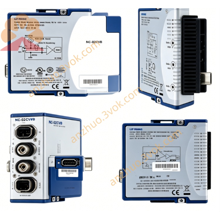
NI PXI‑2598 26.5‑GHz 50‑Ohm Dual‑Transfer PXI RF‑Switch Module
Description
II. Model Interpretation
PXI: Standard PXI bus, only compatible with PXIe hybrid slots and PXI peripheral slots NI.
2598: NI high-frequency RF switch series code, representing dual SPDT (2 groups of 1×2) transmission switches.
Full name: PXI-2598 26.5 GHz 50Ω dual transmission PXI RF switch module NI.
Topology: Two independent SPDT (A/B groups), each group's COM can be switched between NO/NC, used for signal path switching or component insertion / bypass.
III. Technical Parameters
(1) RF Core Characteristics
Frequency range: DC ~ 26.5 GHz (‑3 dB) NI
Characteristic impedance: 50 Ω (full channel matching) NI
Insertion loss: Typical <0.2 dB (26.5 GHz); repeatability <0.03 dB
Channel isolation: Typical ≥70 dB (1 GHz); ≥55 dB (26.5 GHz)
VSWR: Typical ≤1.2:1 (26.5 GHz); maximum ≤1.3:1
Maximum RF power: 75 W (48.75 dBm) / channel (continuous)
Maximum switching voltage: 60 Vrms / 60 VDC NI
Maximum switching current: 1.25 A (resistive) NI
(2) Switch and Relay
Relay type: Electromechanical latch RF relay, gold-plated beryllium copper contacts
Channel configuration: Dual SPDT (A: COM1→NO1/NC1; B: COM2→NO2/NC2)
Action time: Typical 10 ms; maximum 15 ms
Mechanical life: 2.5×10⁶ times (1 V/10 mA)
Electrical life: 5×10⁵ times (75 W/1 GHz)
Termination: Non-terminated, requires external 50Ω terminator
(3) Scanning and Triggering
Scanning list: Maximum 32000 steps programmable list
Full-channel scanning rate: Maximum 2 times/second NI
Trigger channel: PXI backplane Trigger 0~Trigger 7
Minimum trigger pulse width: 150 ns (disable digital filtering)
(4) Physical and Environmental
Form: Standard 3U PXI single-slot module
Front-end connector: 8×SMA (2 groups of SPDT: 2×COM + 2×NO + 2×NC)
Size: 216 mm × 20 mm × 130 mm
Weight: Approximately 0.30 kg
Power supply: PXI backplane 3.3 V/5 V; typical power consumption 1.5 W (3.3 V) + 2 W (5 V)
Operating temperature: 0 ℃ ~ 55 ℃
Storage temperature: –20 ℃ ~ 70 ℃
Humidity: 5% ~ 85%, no condensation
IV. Interface and Communication Configuration
(1) Front-end RF Interface (SMA)
Fixed topology of dual SPDT
Group A: COM1 (common terminal), NO1 (normally open), NC1 (normally closed)
Group B: COM2 (common terminal), NO2 (normally open), NC2 (normally closed)
Connection example
Path switching: Signal source → COM1 → NO1 → DUT; or COM1 → NC1 → load
Component insertion: Signal chain → COM1 → NO1 → filter → NO2 → COM2 → signal chain; cutting NC can bypass filter
(2) Bus and Software Communication
Bus interface: PXI backplane, only available for PXIe hybrid slots / PXI peripheral slots NI
Driver: NI-SWITCH, compliant with IVI specification Software support: LabVIEW, TestStand, LabWindows/CVI, Python, C, .NET
Basic functions: Hardware recognition, channel status reading, scan editing, trigger configuration, relay life counting NI
Synchronization capability: PXI trigger bus enables multi-module high-precision synchronous switching
V. Core functions
26.5 GHz millimeter-wave wideband switching: Covers DC to millimeter-wave, suitable for 5G/6G, satellite communication, radar high-frequency routing NI.
Dual-channel independent SPDT switching: Two independent 1×2 switches, flexible path switching, component insertion / bypass, load switching.
Ultra-low insertion loss + high isolation: 0.2 dB typical insertion loss + 70 dB isolation, ensuring millimeter-wave signal integrity.
75 W medium power carrying capacity: 75 W continuous power per channel, meeting medium-power RF testing requirements.
Relay life monitoring: Board-mounted counter records on/off times, supports predictive maintenance, reduces unexpected downtime NI.
SMA high-reliability connection: Standard SMA connector, stable connection, suitable for high-frequency test cables.
VI. Application scenarios
Millimeter-wave communication testing: 5G/6G millimeter-wave modules, satellite communication equipment, radar system signal path switching and component testing NI.
RF up-conversion and down-conversion link: PXI RF up-converter high-order harmonic transmission, multi-signal source down-converter routing NI.
General RF testing: Path switching, load switching, filter / amplifier insertion / removal between signal sources, oscilloscopes, spectrum analyzers NI.
Semiconductor high-frequency ATE: Millimeter-wave RF IC, high-speed digital chip testing system signal routing NI.
RF aging testing: Long-term stability testing of medium-power RF devices, multi-channel parallel aging.
VII. Usage and Maintenance Instructions
(1) Installation and Power On
Only install in PXIe mixed slots or PXI peripheral slots, do not insert into pure PXIe slots NI.
Before installation, turn off the power, fully insert the module and tighten the panel screws.
After powering on, confirm in NI MAX that the device is recognized normally and there are no errors NI.
(2) Connection and Operation
Use 50Ω SMA cables, recommended torque 0.8~1.0 N・m, avoid over-tightening.
For high-power applications (>50 W), it is recommended to connect an 50Ω load for the unselected channels to prevent open-circuit reflection.
Before switching, confirm that the signal power is within the 75 W rated range to prevent relay contact burnout.
Programming control: Use NI-SWITCH API to configure channels, scan lists and triggers.
(3) Maintenance and Lifespan
Regularly read the relay on/off times through NI MAX, replace when approaching the lifespan value (mechanical 2.5×10⁶ / electrical 5×10⁵) in advance NI.
Maintain ventilation and cooling, do not exceed 55 ℃ working temperature, avoid accelerating aging due to high temperature.
Avoid frequent over-power and over-voltage switching to prevent contact burnout.
When not in use for a long time, store in a dry environment (-20 ℃~70 ℃), avoid oxidation of contacts due to moisture.
Get a Quote