
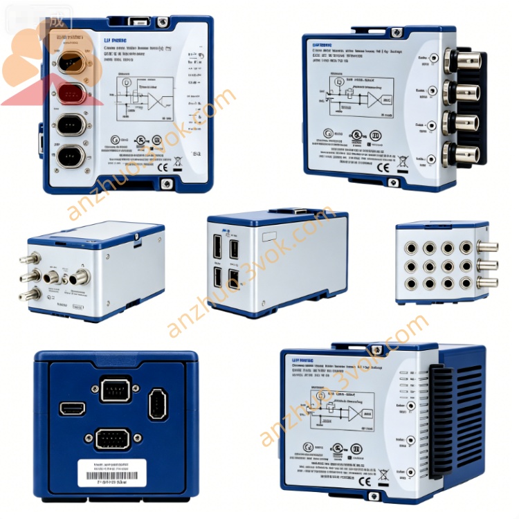
NI PXIe-6548 200MHz 32CH Digital Waveform Instrument
The PXIe-6548 is a 32-channel single-ended bidirectional digital waveform generator/analyser developed by NI. It is a 3U single-slot PXIe module and belongs to the 654x series of 200 MHz high-performance versions. It is specifically designed for high-speed digital interface testing, protocol verification, timing margin and bit error testing, providing higher bandwidth and larger memory configuration from NI.
Description
Product Description
The PXIe-6548 is a 3U single-slot PXIe dual-directional digital waveform generator and analyzer from National Instruments. It belongs to the 654x series, featuring 32 single-ended channels, a maximum operating clock of 200 MHz for SDR mode and 400 MHz for DDR mode. Equipped with built-in hardware comparison function and large on-board memory, it is designed for high-speed digital interface testing, bit error rate testing, protocol verification and timing margin validation scenarios.
Model Definition
PXIe refers to the PXI Express modular bus with Gen1 ×4 specification and single-slot layout. The model number 6548 stands for the high-performance version of the 6500 series digital instrument, which supports 200 MHz SDR and 400 MHz DDR rate, integrates hardware comparison function and is not equipped with parameter measurement unit. Its core features include dual-directional I/O, high-speed data transmission, multi-level voltage support and multi-module synchronous operation.
Key Specifications
Channel and Electrical Characteristics
It has 32 single-ended dual-directional channels, and each channel can be independently set as input or output. The logic voltage levels are software configurable including 1.2 V, 1.5 V, 1.8 V, 2.5 V and 3.3 V. The input voltage range is from -1 V to +4 V, and each channel provides 24 mA output drive current. The output voltage resolution is 100 mV and the input voltage resolution is 50 mV.
Timing and Performance
The maximum clock frequency reaches 200 MHz in SDR mode and 400 MHz in DDR mode, with a top data rate of 400 Mbit/s. Three memory configurations are available: 1 Mbit per channel, 8 Mbit per channel and 64 Mbit per channel. The module adopts an 800 MHz VCO combined with 32-bit DDS clock circuit, achieving 0.2 Hz clock resolution and ±150 ppm frequency accuracy. The channel-to-channel jitter is no more than 1 ns, and it supports synchronous work among multiple modules and multiple chassis. The built-in hardware comparison function supports bit-by-bit comparison, mask configuration, error counting and automatic stop when errors occur, to meet bit error testing requirements.
General Specifications
The overall dimension follows standard 3U PXI form factor. The total weight is approximately 519 grams. Typical power consumption is 32.2 W with maximum power consumption up to 33.5 W. The operating temperature range is 0 °C to 55 °C for standard industrial use.
Interface and Communication Configuration
Host Bus Interface
It adopts PXIe Gen1 ×4 bus, supporting plug-and-play and DMA high-speed data transmission. The maximum input throughput is 660 MB/s and the maximum output throughput is 400 MB/s. It is compatible with PXI trigger bus and RTSI real-time synchronization signal, to realize accurate timing alignment between different modules.
Front Panel Interfaces
A 68-pin VHDCI connector is arranged on the front panel, which integrates all 32 digital I/O signals, strobe signals and event triggers. Three SMA ports are reserved separately. The CLK IN port is for external reference clock input within 5 MHz to 200 MHz. The CLK OUT port is used to output reference clock signals. The PFI 0 port serves as a programmable trigger and event input and output terminal.
Driver and Software Communication
The dedicated driver is NI-HSDIO with IVI compatibility. It can work with NI-MAX for hardware recognition, self-test and parameter configuration. Secondary development is supported on LabVIEW, C/C++, Python and TestStand environments, providing complete application programming interfaces for waveform editing, sequence arrangement and timing configuration.
Core Functions
It realizes synchronous generation and acquisition of high-speed waveforms via 32 independent dual-directional channels, adapting to various parallel digital test tasks. Multiple standard voltage levels can be switched by software to match mainstream low-voltage digital chips. The large-capacity on-board memory supports storage and playback of ultra-long test sequences and reduces reliance on bus transmission. The hardware real-time comparison function completes bit error detection and protocol verification efficiently. The high-precision clock system ensures excellent timing performance and low jitter. The whole device supports multi-module and multi-chassis synchronization to build large-scale parallel test systems.
Application Scenarios
It is widely used in high-speed digital interface testing for DDR, SPI, I²C, UART and LVCMOS buses, as well as bit error rate testing and protocol verification. In semiconductor industry, it conducts functional test and timing verification for memory chips and logic devices. It is also applied to function verification, stimulus generation and response capture of FPGA and MCU. Besides, it completes signal integrity test for high-speed interfaces of display panels and image sensors, and carries out timing synchronization and reliability evaluation for digital systems in aerospace and military fields.
Usage and Maintenance Instructions
Usage Guidelines
Install the module into a free slot of standard 3U PXIe chassis and fasten the fixing screws. Use matched shielded cables for signal connection, and control the cable length within 1 meter under high-speed working conditions. Adopt 50 ohm coaxial cables for SMA clock ports to avoid signal reflection. Complete channel direction, voltage level, clock frequency and trigger settings through configuration software, and set waveform sequences and comparison parameters according to test demands. Calibrate the reference clock in advance when conducting multi-device synchronous tests.
Maintenance Instructions
Clean the front panel and connectors regularly with dry soft cloth and keep the device away from liquid. This digital module does not require frequent calibration. It is recommended to inspect output voltage, drive current and timing performance every two years. When the module is not in use, store it in a dry environment with temperature between -20 °C and 60 °C and relative humidity below 60%, and take anti-static protection measures. If abnormal operation occurs, firstly check wiring, power supply and software configuration. Inspect cables and grounding status for timing faults, and check whether the load is short-circuited or overloaded for output anomalies.
Get a Quote