
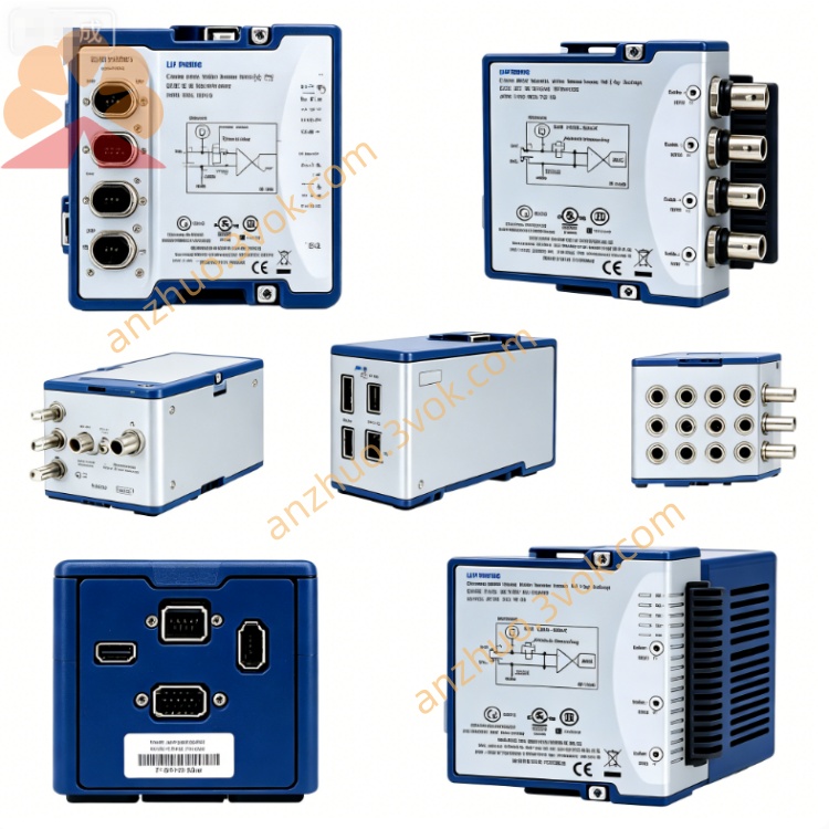
NI PXIe-6545 200MHz 32CH Digital Waveform Instrument
Description
PXIe‑6545 Product Introduction
PXIe‑6545 (Part Number 780993‑02/03) is a 32-channel, 200 MHz, single-ended bidirectional digital waveform generator/analyser from NI, a 3U single-slot PXIe module, representing the high-frequency upgrade version of NI 6544. Equipped with high-performance FPGA, each channel comes standard with 1 Mbit, and the high-end version has 64 Mbit onboard memory. It supports 1.2–3.3 V multi-level, 5 ns timing accuracy, and complex mode generation/collecting, targeting high-performance testing scenarios such as high-speed digital chips, semiconductors, and display panels.
Model Interpretation
PXIe: PXI Express bus, 3U size, Gen1 x4, single-slot exclusive bandwidth, supports DMA, RTSI, and PXI trigger.
6545: 6500 series 200 MHz, 32-channel, single-ended, high-frequency standard version, without hardware comparison and PMUNI.
Core Identification: Bidirectional I/O, 200 MHz, large-capacity memory, multi-level, nanosecond-level timing, multi-module synchronization. Technical Specifications
Channels and Electricals
Channel: 32 single-ended bidirectional I/O, each channel has independent input/output configuration by NI.
Logic level: Software selectable from 1.2 V, 1.5 V, 1.8 V, 2.5 V, 3.3 V, covering mainstream low-voltage devices by NI.
Input voltage: -1 V to + 4 V; Output drive: Each channel 24 mA NI.
Signal type: Single-ended, non-differential by NI.
Timing and Performance
Maximum clock: 200 MHz (single cycle 5 ns) by NI.
Data rate: 200 Mbit/s (same generation/collecting speed).
Onboard memory: Standard version 1 Mbit/channel (total 4 MB), high-end version 64 Mbit/channel (total 256 MB).
Clock system: 800 MHz VCO + 32-bit DDS, resolution 0.2 Hz, accuracy ±150 ppm download.ni.com.
Synchronization: Multi-module/multi-rack synchronization, channel-to-channel jitter ≤ 1 ns, output setup/hold time 5 ns.
General Specifications
Bus: PXIe Gen1 x4, single slot, DMA throughput: input 660 MB/s, output 400 MB/s.
Connectors: Front panel 68-pin VHDCI (DDC) + 3 SMA (CLK IN, CLK OUT, PFI0) by NI.
Power consumption: Typical 32.2 W, maximum 33.5 W (+3.3 V 1.75 A, +12 V 2.2 A) by NI.
Operating temperature: 0 °C to + 55 °C, industrial grade by NI.
Size/Weight: 3U (21.6×2.0×13.0 cm), approximately 519 g by NI.
Interface and Communication Configuration
Host interface: PXIe bus, plug-and-play, DMA high-speed transmission, supports RTSI real-time synchronization and PXI trigger bus, ensuring multi-device timing alignment.
Front panel interface: 68-pin VHDCI (DDC) integrated 32 channels I/O, clock, trigger and event signals; 3 SMA for external clock input/output and PFI trigger, suitable for 200 MHz high-frequency synchronization requirements by NI.
Trigger and Synchronization: Supports software, edge, handshake, mode triggering; can be synchronized with 6544/6547/6548 multi-modules, aligning timing through 100 MHz base clock.
Driver software: NI-HSDIO (compatible with IVI), combined with LabVIEW, C/C++, Python, TestStand, providing waveform editing, mode sorting and timing configuration APIs; NI-MAX for hardware configuration. Core function
32-channel bidirectional high-speed waveform generation / acquisition: Each channel is independently configured, synchronously generating excitation and acquisition responses, suitable for parallel testing with NI.
Flexible multi-level adaptation: Software switching from 1.2 V to 3.3 V, covering mainstream low-voltage digital devices, without the need for hardware modifications from NI.
Large-capacity onboard memory: High configuration of 64 Mbit per channel, supporting ultra-long sequence mode storage and playback, reducing bus dependence.
High-precision clock and timing: DDS with low jitter clock, channel-to-channel jitter ≤ 1 ns, output setup / hold time 5 ns, meeting strict timing tests.
Flexible mode sequencing and triggering: Supports multi-waveform sequences, loops, conditional branches, enriching trigger sources to adapt to complex test processes.
Mixed-signal system integration: Can be synchronized with PXIe oscilloscopes and arbitrary waveform generators to build a complete digital-analog mixed test system. Applicable scenarios
High-speed digital chip verification: Function testing of FPGA, MCU, high-speed interface chips (such as DDR, SPI, I²C), protocol simulation, timing verification.
Semiconductor testing: Pattern generation/capture of high-speed memory and logic devices, production function testing and timing verification with NI.
Display and image testing: Digital interface testing and signal integrity verification of high-speed LCD/OLED panels, CMOS/CCD image sensors.
Embedded system testing: High-speed bus simulation of embedded devices, peripheral interface testing, firmware function verification.
Aerospace / Military: High-speed digital signal synchronous acquisition in strong interference environment, multi-device timing linkage, weapon system I/O control and status monitoring.
User and maintenance instructions
Key usage points
Installation: Insert into a single slot of a 3U PXIe chassis, tighten the screws, recommend using high-performance chassis such as PXIe-1085 to ensure power supply and heat dissipation.
Cabling: Use the matching SHC68-C68-D4 shielded cable. For 200 MHz high-frequency, the cable length should be ≤ 1 m; for SMA clock lines, select 50 Ω coaxial cables to reduce signal reflection.
Configuration: Set the channel direction, level, clock frequency, and trigger mode in NI-MAX; configure the mode sequence, timing parameters, and synchronization function in NI-HSDIO.
Timing considerations: Strictly control the cable length and grounding in high-frequency applications to avoid crosstalk; calibrate the reference clock before synchronous testing.
Maintenance and calibration
Cleaning: Regularly wipe the panel and connectors with a dry soft cloth to remove dust and prevent liquid contact.
Calibration: Digital I/O does not require regular calibration; it is recommended to check the output level, drive current, and timing accuracy every 2 years.
Storage: When not in use for a long time, store in a dry environment at -20 °C to + 60 °C with a humidity of ≤ 60%, and take anti-static protection measures.
Troubleshooting: Check wiring, power supply, and software configuration first when there is an anomaly; check the cable and grounding for timing anomalies; check the load for output anomalies if it is overloaded or short-circuited.
Get a Quote