
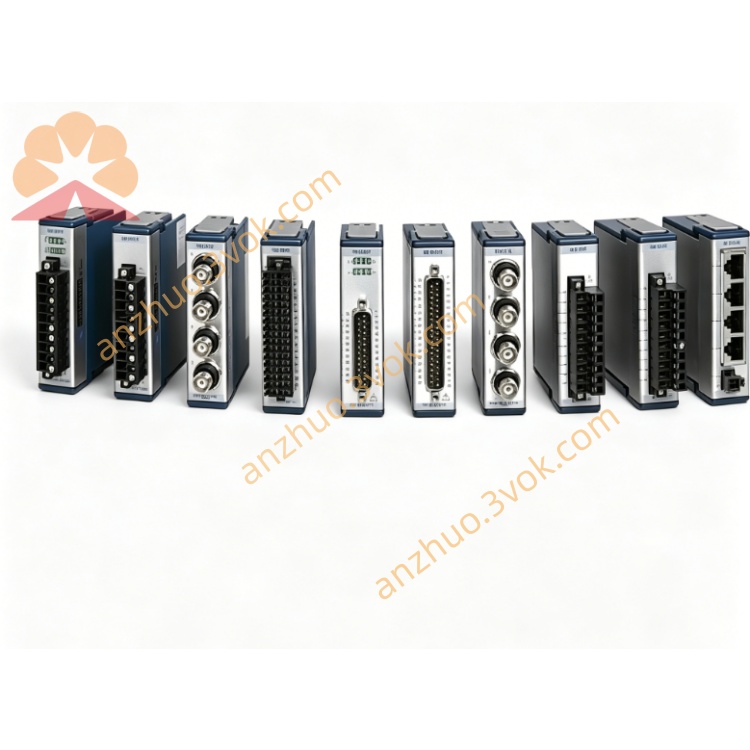
NI PXIe-6537 50MHz 32CH High-Speed Digital I/O Module
Description
Model Explanation
PXIe: Based on the PXI Express bus, 3U specification, Gen1 x4 link, exclusive bandwidth per slot, supports multi-rack synchronization and high-speed DMA transmission.
6537: The NI high-speed bidirectional I/O series number, representing the highest performance configuration of 32 channels, 50 MHz, 200 MB/s.
Core Identifier: Bidirectional programmable I/O, 50 MHz clock, 200 MB/s throughput, multi-level compatibility, independent control per channel direction, streaming data transmission. Technical Specifications
Channels and Electrical Characteristics
Channel: 32 bidirectional digital I/O, each channel can be independently configured as input or output NI.
Logic Level: Software selectable 2.5 V, 3.3 V, 5 V TTL, compatible with mainstream digital devices.
Input Voltage Range: -1 V to + 6 V; Output Voltage Range: 0 V to 5 V.
Single Channel Drive Capacity: 32 mA, capable of directly driving TTL loads, relays, and small actuators.
Timing and Performance
Maximum Working Clock: 50 MHz, single cycle 20 ns, sampling accuracy 10 ns.
Data Throughput: 200 MB/s (32 bit × 50 MHz), supports PXIe continuous streaming transmission.
Channel-to-Channel Jitter: ≤ 1.2 ns; Output Setup Time Deviation: ≤ 1.5 ns, excellent timing consistency.
Synchronous Reference: 100 MHz differential reference clock, supports multi-module, multi-rack precise synchronization.
General Specifications
Bus Interface: PXIe Gen1 x4, single slot, supports DMA, RTSI trigger and PXI trigger bus.
Connector: Front panel 68-pin VHDCI shielded interface, paired with SHC68-C68-D4 shielded cable.
Power Consumption: +5 V approximately 2.5 A, total power consumption approximately 12.5 W.
Operating Temperature: 0 °C to + 55 °C, industrial-grade wide temperature design, suitable for harsh environments.
Size and Weight: 3U PXI specification, approximately 21.6 × 2.0 × 13.0 cm, weight approximately 160 g.
Interface and Communication Configuration
Host Interface: Using PXIe bus, plug-and-play, supports high-speed data transmission via DMA, real-time synchronization via RTSI trigger and PXI trigger bus, ensuring timing alignment of multiple devices.
Front Panel Interface: 68-pin VHDCI shielded connector, integrates all I/O signals, power supply, and grounding, has strong anti-electromagnetic interference capability, paired with dedicated shielded cable to reduce signal attenuation.
Trigger and Synchronization: Supports software trigger, edge trigger, handshake trigger; can be synchronized with PXIe-6535/6536 modules for multiple devices, and aligns timing between multiple racks via 100 MHz base clock.
Driver Software: Standard NI-DAQmx driver, compatible with Windows and real-time operating systems, supports development environments such as LabVIEW, C/C++, Python, TestStand, simplifying programming and configuration. Core function
32-channel bidirectional programmable I/O: Each channel can be independently configured as input or output, enabling flexible implementation of signal acquisition and driving, suitable for high-density parallel testing requirements from NI.
Multi-level compatibility: Software can switch between 2.5 V, 3.3 V, and 5 V TTL levels, without the need for hardware modifications to adapt to different voltage standards of digital chips.
Ultra-fast streaming transmission: 50 MHz clock, 200 MB/s throughput, supports continuous large data stream transmission, meeting scenarios such as high-speed image data acquisition and display panel timing verification.
Precise timing synchronization: 100 MHz base clock, channel-to-channel jitter ≤ 1.2 ns, multi-module synchronization ensures nanosecond-level timing consistency.
Input filtering and change detection: Programmable debouncing function, supports edge triggering and level change detection, reduces CPU usage and improves signal acquisition stability from NI.
High driving capability: Single channel 32 mA driving current, can directly drive TTL loads, relay arrays, and small actuators, without the need for additional driving circuits. Applicable scenarios
Semiconductor testing: High-speed parallel Pattern generation and capture for memory and logic devices, chip protocol simulation, functional verification and mass production testing. NI.
Image / Display testing: High-speed data acquisition for CMOS/CCD image sensors, timing control for LCD/OLED display panels and signal integrity verification. NI.
High-speed digital communication: High-speed protocol simulation, bus monitoring, and device handshake interaction testing for SPI, UART, I²C, etc. NI.
Industrial automation: High-density high-speed acquisition of switch quantities, high-speed relay array control, and parallel signal synchronization testing of production lines. NI.
Aerospace / Military: High-speed digital signal synchronization acquisition in strong interference environments, multi-device timing linkage, and I/O control and status monitoring of weapon systems. NI.
User and Maintenance Instructions
Key Usage Points
Installation: Insert into a single slot of a 3U PXIe chassis, lock and fix the screws, and it is recommended to pair with high-performance chassis such as PXIe-1071, PXIe-1085 to ensure power supply and heat dissipation.
Cabling: Use SHC68-C68-D4 shielded cables to connect the equipment, separate strong and weak signals for wiring to avoid common ground interference; in 50 MHz high-speed scenarios, the cable length is recommended to be ≤ 1 m to reduce signal attenuation and jitter.
Configuration: Set the channel direction, logic level, working clock, input filtering and trigger mode through NI-MAX or DAQmx software, and configure the synchronization parameters of multiple modules as needed.
Timing Considerations: For high-frequency (≥ 20 MHz) applications, strictly control the cable length and wiring path to avoid signal reflection and crosstalk; calibrate the 100 MHz reference clock before synchronous testing.
Maintenance and Calibration
Cleaning: Regularly wipe the panel and connectors with a dry soft cloth to remove dust and oxide layers, avoid contact with liquids, and prevent short circuits or corrosion.
Calibration: Digital I/O modules do not require regular calibration. It is recommended to check the output level, drive current and timing accuracy once every 2 years to ensure performance meets the specifications.
Storage: When not in use for a long time, place the equipment in a dry environment of -20 °C to + 60 °C with a humidity of ≤ 60%, take anti-static protection measures, and avoid damage from static electricity to the FPGA and interface circuits.
Troubleshooting: When encountering abnormalities, first check if the wiring is firm, if the power supply is stable, and if the software configuration is correct; for timing abnormalities, check the cable quality and grounding design; for output abnormalities, check if the load is overloaded or short-circuited.
Get a Quote