
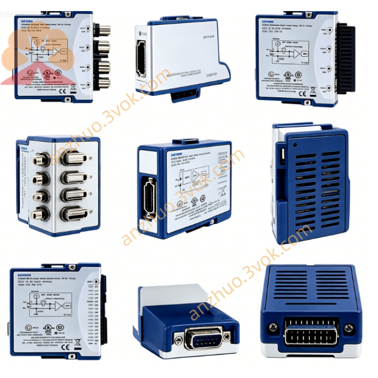
NI PXIe-5840 6GHz 1GHz BW RF Vector Signal Transceiver
Description
Model Definition
PXIe: PXI Express high‑speed modular bus
58: NI second‑generation VST series
40: RF‑centric model, 9 kHz–6 GHz, 1 GHz bandwidth
VST: Vector Signal Transceiver (integrated TX + RX + FPGA + DIO)
Key variant: 2‑slot, 3U, Virtex‑7 FPGA, 1 GHz RF I/Q bandwidth
Key Specifications
Generator (TX)
Frequency range: 9 kHz to 6 GHzNI
Instantaneous bandwidth: Up to 1 GHz (≥2.2 GHz)NI
Max output power: +20 dBm (typical)
Tuning time: 300 µs (typical)
Resolution: 16‑bit DACNI
Analyzer (RX)
Frequency range: 9 kHz to 6 GHzNI
Instantaneous bandwidth: Up to 1 GHz (≥2.2 GHz)NI
Input range: –70 dBm to +10 dBm
EVM: <–50 dB (802.11ax, loopback)
Resolution: 14‑bit ADC, dual‑channelNI
FPGA & Memory
FPGA: Xilinx Virtex‑7 VX690T (user‑programmable)NI
Onboard DRAM: 2 × 2 GB
Onboard SRAM: 2 MB
General
Module size: 2‑slot, 3U PXIe
Operating temperature: 0 °C to 55 °C
Calibration interval: 2 years
Power consumption: ~80 W
Interface & Communication Configuration
Host bus: PXI Express Gen 2, compatible with PXIe chassis
RF I/O: 1 × SMA RF OUT (TX), 1 × SMA RF IN (RX), 50 Ω
Baseband I/Q: 2 × SMA differential I/Q (I+, I−, Q+, Q−)
Reference clock: 10 MHz REF IN/OUT (SMA)
Trigger: PXI trigger bus, external TRIG IN/OUT (SMA)
Digital I/O: 8‑port parallel DIO (60 MHz), 4‑port high‑speed serial (12 Gb/s)
Control software: NI‑RFSG, NI‑RFSA, LabVIEW, LabWindows/CVI, C#, Python
Synchronization: NI‑TClk, PXI star trigger, multi‑module phase alignment
Core Functions
Integrated RF generation & analysis: Combines wideband RF TX/RX for closed‑loop RF testing without external instruments.
1 GHz ultra‑wideband RF capability: Supports 5G NR, Wi‑Fi 6/7, and radar wideband signal validation.
User‑programmable FPGA: Enables real‑time processing (filtering, FFT, modulation/demodulation, DPD) via LabVIEW FPGA.
High‑accuracy RF performance: <–50 dB EVM and ±0.5 dB amplitude accuracy for high‑order modulation.
MIMO‑ready synchronization: NI‑TClk enables multi‑module phase alignment for 4×4/8×8 MIMO.
Envelope tracking & DPD: Optimizes PA efficiency/linearity for 5G and LTE applications.
Applications
Wireless device test: 5G NR, LTE‑A Pro, Wi‑Fi 6/7, and IoT transceiver validation.
RFIC & SoC test: High‑speed RF chipset characterization and jitter analysis.
Radar & EW: Wideband signal generation/analysis for radar prototyping and electronic warfare.
Aerospace & defense: Precision RF testing for avionics and military communications systems.
Power amplifier test: Envelope tracking, DPD, and linearity characterization for RF PAs.
Usage & Maintenance
Installation: Insert into 2 consecutive 3U PXIe chassis slots; connect RF IN/OUT to DUT, 10 MHz reference, and triggers.
Warm‑up: 30 minutes at ambient temperature before high‑accuracy measurements.
Operation: Configure frequency, power, bandwidth, and triggering via software; avoid input overvoltage (>+10 dBm) and ESD.
Cable care: Use high‑quality 50 Ω SMA cables; inspect connectors for wear/dirt periodically.
Maintenance: Keep SMA connectors clean/dry; ensure chassis cooling airflow is unobstructed.
Calibration: Self‑calibrate monthly; factory calibrate every 2 years to maintain RF accuracy.
Get a Quote