
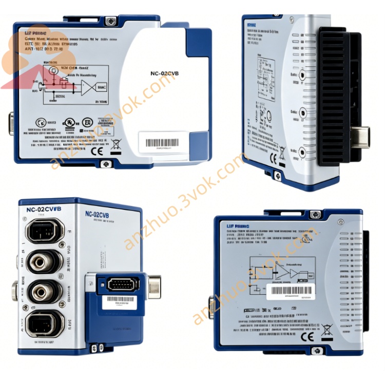
NI PXIe-5774 FlexRIO 6.4GS/s Digitizer Module
Description
Model Definition
PXIe: PXI Express high‑speed modular bus
57: NI FlexRIO series (reconfigurable FPGA‑based instruments)
774: 2‑channel, 6.4 GS/s, 3 GHz bandwidth digitizer
FlexRIO: FPGA‑programmable I/O for custom instrumentation
Key variant: DC‑coupled, 12‑bit resolution, Kintex UltraScale FPGA
Key Specifications
Channels: 2 single‑ended, simultaneous sampling
Resolution: 12 bits
Max sample rate: 6.4 GS/s (single‑channel interleaved); 3.2 GS/s (dual‑channel)
Analog bandwidth: DC to 3 GHz (–3 dB)
Input coupling: DC
Voltage ranges: 200 mVpp, 1 Vpp (software‑selectable, with DC offset)
Input impedance: 50 Ω (SMA female)
Max input power: +10 dBm (continuous)
Onboard memory: 4 GB DRAM (2 × 2 GB banks)
FPGA: Xilinx Kintex UltraScale (KU040/KU060 options)
Data interface: PXIe Gen 1, up to 4 GB/s throughput
Trigger: External TRIG IN/OUT (SMA), PXI backplane trigger
Reference clock: 10 MHz REF IN/OUT (SMA)
Operating temperature: 0 °C to 55 °C
Calibration interval: 2 years
Interface & Communication Configuration
Host bus: PXI Express Gen 1, compatible with PXI/PXIe chassis
Analog inputs: 2 × SMA female (AI 0, AI 1), 50 Ω
Clock/reference: 1 × SMA (REF/CLK IN)
Trigger: 1 × SMA (TRIG IN), 1 × SMA (TRIG OUT)
FPGA I/O: 8 bidirectional DIO channels (via CLIP interface)
Control software: FlexRIO driver, LabVIEW, LabWindows/CVI, C#, Python
Synchronization: NI‑TClk, PXI star trigger, multi‑module phase alignment
Core Functions
High‑speed waveform acquisition: Captures DC‑to‑3 GHz signals at up to 6.4 GS/s for ultra‑wideband RF and time‑domain measurements.
Dual‑channel simultaneous sampling: Enables phase‑coherent multi‑channel acquisition for differential or MIMO systems.
User‑programmable FPGA: Implements custom real‑time processing (filtering, FFT, triggering, decimation) via LabVIEW FPGA.
Large onboard memory: 4 GB DRAM supports long‑duration waveform capture and streaming.
DC‑coupled precision: Direct DC coupling eliminates AC‑coupling distortion, critical for baseband and low‑frequency RF signals.
Flexible triggering: Supports edge, pulse, window, and software triggers; enables synchronized acquisition across multiple modules.
Applications
Wireless communications: 5G NR, LTE, Wi‑Fi 6/7, and ultra‑wideband (UWB) signal capture and analysis.
RF & microwave test: High‑speed transient analysis, pulse characterization, and wideband spectrum monitoring.
Scientific instrumentation: Particle physics, laser diagnostics, and high‑energy physics waveform acquisition.
Medical imaging: Ultrasound, MRI, and high‑speed biomedical signal recording.
Semiconductor test: High‑speed digital/RF IC characterization and jitter analysis.
Usage & Maintenance
Installation: Insert into 3U PXIe chassis; connect SMA inputs to DUT, REF/CLK to 10 MHz reference, and TRIG signals as needed.
Warm‑up: 30 minutes at ambient temperature before high‑accuracy measurements.
Operation: Select sample rate, voltage range, and triggering via software; avoid input overvoltage (>+10 dBm) to prevent damage.
Maintenance: Keep SMA connectors clean and dry; inspect cables periodically; avoid electrostatic discharge (ESD).
Calibration: Perform self‑calibration monthly; factory calibrate every 2 years to maintain accuracy.
Get a Quote