
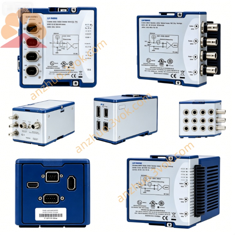
NI PXIe-5673E 6.6GHz RF Vector Signal Generator
Description
Model Definition
PXIe: PXI Express high‑speed modular instrument bus
56: NI PXI RF/microwave test series
73: 6.6 GHz frequency coverage, wide bandwidth vector signal generator
E: Enhanced version with improved tuning, additional reference output, and peer‑to‑peer streaming
Composition: PXIe‑5450/5451 (AWG) + PXIe‑5611 (I/Q modulator) + PXIe‑5650/5651/5652 (LO)
Key Specifications
Frequency range: 50 MHz to 6.6 GHz
Instantaneous bandwidth: Up to 100 MHz (3 dB)
Amplitude range: –145 dBm to +10 dBm
Noise density: –120 dBm/Hz (typical, 0 dBm output)
Dynamic range: 132 dB (compression‑to‑noise)
Phase noise: –105 dBc/Hz @10 kHz offset (1 GHz carrier, typical)
Frequency stability: ±20 ppb (OCXO timebase)
Waveform memory: 32 MB / 256 MB / 512 MB (per channel, optional)
AWG resolution: 16‑bit, 1 GS/s (interpolated)
RF output interface: SMA female, 50 Ω
Max output power: +10 dBm
Reference: 10 MHz (external input, internal OCXO output; REF OUT2 on E version)
Triggering: PXI trigger bus, PXI star trigger, NI‑TClk synchronization
Data streaming rate: 500 MB/s (nominal, peer‑to‑peer supported on E version)
Operating temperature: 0 °C to 55 °C
Calibration interval: 2 yearsNI
Interface & Communication Configuration
Host bus: PXI Express Gen 1, compatible with PXI/PXIe chassis
RF output: SMA female, 50 Ω impedance
Reference connectors: 10 MHz BNC (REF IN, REF OUT, REF OUT2 on E version)
Trigger: PXI backplane trigger lines, star trigger
Synchronization: NI‑TClk for multi‑module phase alignment
Control software: NI‑RFSG driver, compatible with LabVIEW, LabWindows/CVI, C#, Python
Module interconnections: Internal cabling between AWG, I/Q modulator, and LO
Core Functions
Vector signal generation: Creates standard and custom modulated signals including AM, FM, CPM, ASK, FSK, MSK, PSK, QAM (4/16/64/256), multitone, and arbitrary waveforms.
Wideband I/Q modulation: Integrated I/Q modulator supports up to 100 MHz instantaneous bandwidth for 5G, Wi‑Fi 6/7, and broadband IoT.
High‑purity signal output: Low phase noise and high frequency stability ensure accurate RF device characterization.
Enhanced features (E version): RF list mode, faster tuning, additional REF OUT2, peer‑to‑peer streaming.
Software‑defined operation: Switch modulation types and customize waveforms via software; supports stream‑from‑disk for continuous terabyte‑level waveforms.
Multi‑module synchronization: NI‑TClk enables phase‑coherent multi‑channel test systemsNI
Applications
Wireless communication: R&D and production test of 5G, LTE, Wi‑Fi 6/7, Bluetooth 5, and IoT modules/terminals.
RF components: Amplifiers, filters, mixers, and front‑end module performance validation.
Semiconductor: RF ICs, transceivers, and SoC testing.
Aerospace & defense: Radar signal simulation, electronic warfare, and satellite communication test.
General RF: RFID, software‑defined radio (SDR), and wireless sensor network testingNI
Usage & Maintenance
Installation: Install all three modules in adjacent 3U PXI/PXIe chassis slots; connect internal IF/RF cables; connect 10 MHz reference and trigger signals.
Warm‑up: Allow 30 minutes warm‑up at ambient temperature before high‑accuracy measurements.
Operation precautions: Avoid short‑circuiting the RF output; maximum output power is +10 dBm to prevent front‑end damage.
Maintenance: Keep SMA connectors clean; inspect cables periodically; calibrate every 2 years.
Safety: Module surface may become hot during operation; allow cooling before handling or removal
Get a Quote