
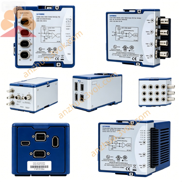
NI PXIe-5653 RF LO Synthesizer Module
Description
Model Nomenclature
PXIe: PXI Express high-speed modular instrumentation bus.
56: NI PXI RF/IF test & measurement series.
53: High-stability LO synthesizer with dual OCXO references.
Technical Specifications
Form Factor: 3U, 2‑slot PXIe module.
Frequency Outputs:
LO1: 3.2 GHz to 8.3 GHz (nominal), SMA 50 Ω.
LO2: 4.0 GHz (fixed), SMA 50 Ω.
LO3: 800 MHz (fixed), SMA 50 Ω.
Reference Clocks:
REF IN: 10 MHz, 2 Vpk‑pk max, SMA.
REF OUT (10 MHz): From onboard OCXO.
REF OUT (100 MHz): From onboard OCXO.
Phase Noise: Typically <‑130 dBc/Hz @ 10 kHz offset (1 GHz carrier).
Frequency Resolution: 0.001 Hz.
Settling Time: Fast locking for frequency hopping.
Power Consumption: +12 VDC, 1.10 A (3.63 W) typ; 4.00 A (48.00 W) maxNI.
Calibration Interval: 2 yearsNI.
Temperature: Operating 0 °C to 55 °C; Storage –40 °C to 70 °C.
Front Panel Connectors
REF IN: External 10 MHz reference input.
REF OUT (10 MHz): 10 MHz OCXO reference output.
REF OUT (100 MHz): 100 MHz OCXO reference output.
LO1 OUT: 3.2–8.3 GHz LO output (to PXIe-5606).
LO2 OUT: 4.0 GHz LO output.
LO3 OUT: 800 MHz LO output.
LEDs: ACCESS (status), LOCK (PLL lock indicator).
Core Features
High‑Purity LO Signals: Low phase noise for accurate RF downconversion and modulation analysis.
Dual OCXO References: 10 MHz and 100 MHz oven‑controlled oscillators for excellent frequency stability.
Wide LO Coverage: LO1 covers 3.2–8.3 GHz, supporting S‑ to X‑band radar and microwave test.
PXIe Integration: Seamless synchronization with PXIe‑560x downconverters and PXIe‑562x digitizers.
Fast Switching: Rapid frequency settling for swept‑tuned and hopping applications.
Application Scenarios
High‑Speed VSA Systems: PXIe‑5665/5668 RF vector signal analyzers.
Radar Test: LO generation for S‑band (2–4 GHz) and X‑band (8–12 GHz) radar signal analysis.
Electronic Warfare (EW): Low‑noise LO for signal interception and spectrum monitoring.
Semiconductor RF Test: Local oscillator for transceiver and power amplifier characterization.
Aerospace & Defense: Precision LO for satellite communication and SIGINT systems.
Get a Quote