
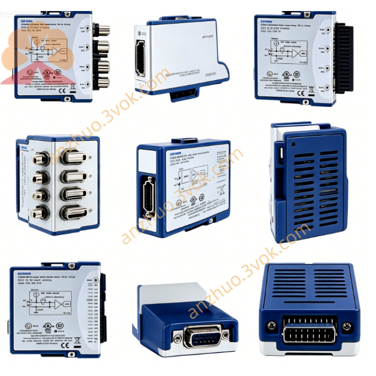
NI PXIe-5645R 6GHz Reconfigurable RF Vector Signal Transceiver
Description
Model Nomenclature
PXIe: PXI Express high‑speed modular instrumentation bus.
56: NI PXI RF/IF test & measurement series.
45: 6 GHz frequency, 80 MHz bandwidth, extended baseband I/Q, 4‑slot form factor.
R: Reconfigurable (user‑programmable FPGA via LabVIEW FPGA).
Technical Specifications
Form Factor: 4‑slot 3U PXIe module.
Frequency Range: 65 MHz to 6 GHz; <1 Hz tuning resolution.
Instantaneous Bandwidth: 80 MHz (200 MHz optional).
RF Input (VSA): SMA, 50 Ω; noise floor –148 dBm/Hz (typ); IIP3 ≥19 dBm.
RF Output (VSG): SMA, 50 Ω; avg power up to +6 dBm; ACPR ≤–45 dBc.
Baseband I/Q: Differential/single‑ended, 16‑bit, 120 MS/s, 80 MHz complex bandwidth.
FPGA: Xilinx Virtex‑6 LX195T (user‑programmable).
Onboard Memory: 2×256 MB DRAM, 2 MB SRAM.
Digital I/O: 24 channels, up to 250 Mbit/s.
Reference: External 10 MHz (SMA), internal oscillator.
Trigger: PXI trigger bus, external TRIG (SMA, 3.3 V TTL).
Temperature: Operating 0 °C to 55 °C; Storage –40 °C to 70 °C.
Interface and Communication Configuration
Bus: PXIe Gen2 x4, peer‑to‑peer streaming, high‑speed DMA.
Drivers: NI‑5645R, IVI‑COM; compatible with LabVIEW, C/C++, Python, .NET.
Software: NI‑MAX (config), LabVIEW FPGA (custom processing), NI‑RFmx (standard measurements).
Synchronization: PXI trigger bus, NI‑TClk for multi‑module phase alignment.
I/O Connectors: 1×RF IN (SMA), 1×RF OUT (SMA), 1×10 MHz Ref In/Out (SMA), 1×TRIG (SMA), 24×Digital I/O, Baseband I/Q (differential/single‑ended).
Core Features
Integrated VSA/VSG + Baseband I/Q: Test RF and baseband signals with one instrument.
User‑Programmable FPGA: Real‑time filtering, modulation/demodulation, protocol decoding, and custom DSP.
Wideband RF Performance: 80 MHz bandwidth, 6 GHz coverage for 5G/LTE/Wi‑Fi 6/7/radar.
High Dynamic Range: Low noise floor and high linearity for accurate weak/strong signal measurement.
MIMO‑Ready: FPGA‑based synchronization enables multi‑module MIMO configurations.
Application Scenarios
Wireless R&D & Test: 5G/6G, LTE‑A, Wi‑Fi 6/7, Bluetooth, and RFID device validation.
RF + Baseband Test: Transceiver characterization, power amplifier/filter test, and baseband I/Q validation.
Aerospace & Defense: Radar signal generation/analysis, EW simulation, SIGINT.
Semiconductor Test: RFIC/transceiver ATE, high‑speed digital I/O, and protocol validation.
Software‑Defined Radio (SDR): Custom waveform prototyping, beamforming, and adaptive communications.
Get a Quote