
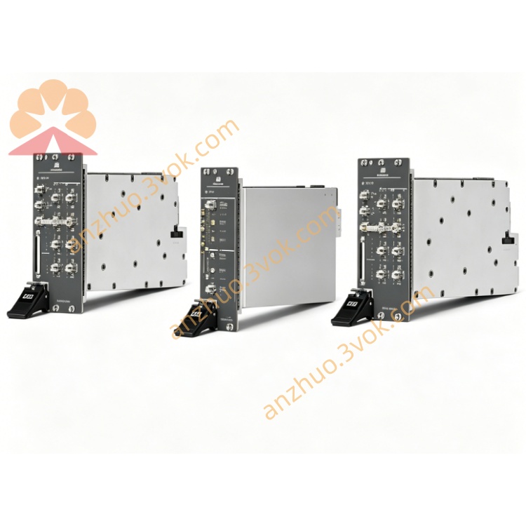
NI PXI‑5695 8‑GHz Programmable RF Attenuator Module
Description
II. Model Interpretation
PXI: Compliant with the PXI industrial bus standard, 3U shape, single slot, compatible with PXI/PXIe chassis.
5695: NI RF signal conditioning series model, representing an 8 GHz bandwidth, dual-channel programmable RF attenuator.
Part Number: 781036-01 (standard model).
III. Technical Parameters (25℃, 50 Ω, preheating 10 min)
1. Frequency and Channels
Frequency range: 50 MHz to 8 GHz
Number of channels: 2 channels (CH0 fixed attenuation, CH1 programmable attenuation)
2. Attenuation Characteristics
CH0 (fixed): Main path 30 dB; bypass path 0 dB (bypass)
CH1 (programmable): Attenuation range 0 to 40 dB, step size 0.5 dB
Total attenuation (cascade): Maximum 70 dB (2.5 GHz)
Attenuation accuracy: ±0.7 dB; stabilization time: ≤ 4 μs
3. Power and Impedance
Maximum input power (operating): +27 dBm (CH1), +33 dBm (CH0)
No damage limit input power: +33 dBm
Output impedance: 50 Ω; typical VSWR: 1.3:1
4. Physical and Environmental
Size: 3U, single slot (21.6 cm × 2.0 cm × 13.0 cm)
Weight: 263 g
Operating temperature: 0 to 55℃; humidity: 10% to 90% (no condensation)
Power consumption: Powered by PXI backplane
IV. Interface and Communication Configuration
Front panel interface (SMA female connector, 50 Ω, AC coupling)
CH0 IN/OUT: Fixed attenuation channel input/output (including main path and bypass path)
CH1 IN/OUT: Programmable attenuation channel input/output
Indicators: Power, lock, fault status
Bus and Software
Backplane: Standard PXI bus (PCI, trigger, 10 MHz reference)
Driver: NI-5690, supports LabVIEW, TestStand, Python, C#
Synchronization: Supports multi-module clock and trigger synchronization
V. Core Functions
Dual-channel independent attenuation: CH0 provides fixed 30 dB or bypass, CH1 wide-range programmable, suitable for high-power and small-signal scenarios.
Wideband high precision: Full coverage from 50 MHz to 8 GHz, 0.5 dB fine step, high attenuation accuracy, ensuring signal power accuracy.
Large dynamic range: Maximum 70 dB attenuation cascade, significantly expands VSG dynamic range, meeting receiving sensitivity testing requirements.
High power tolerance: CH0 can withstand +33 dBm input, suitable for large-power signal link attenuation.
System-level integration: Can replace traditional switch attenuation network, simplifies test system architecture, improves stability.
VI. Application Scenarios
Wireless communication testing: Bluetooth, Wi-Fi, 5G RF module receiving sensitivity testing, precise control of input power.
RF component testing: Amplifier, filter, mixer attenuation/damage/linearity verification.
Radar and electronic warfare: Radar signal power adjustment within 8 GHz, simulating signal path loss.
Aerospace / Defense: Military RF equipment calibration, large-power signal attenuation, small-signal precise control.
Automotive electronics: Vehicle radar, tire pressure monitoring, Bluetooth, etc. RF component testing.
VII. Usage and Maintenance Instructions
Installation and Power On
Power off and install to a single slot, chassis reliably grounded; preheat for 10 minutes and self-check.
During operation, keep the air duct unobstructed, environmental temperature ≤ 55℃, avoid blocking the fan.
Wiring and Operation The RF interface uses 50 Ω SMA cable with tightened anti-reflection; the input power should not exceed the rated value.
When multiple modules are synchronized, a common 10 MHz reference clock and trigger signal are used.
Reasonably set the attenuation value of CH1 to avoid overload of the subsequent stage due to too small value.
Daily maintenance and calibration
Perform traceability calibration once a year to compensate for parameter deviations caused by long-term use; built-in self-calibration corrects temperature drift.
Clean the SMA interface regularly, install a dust cap for long-term inactivity; keep the environment free of condensation and strong vibrations.
Do not plug or unplug the cable while powered on to avoid electrostatic shock (the interface is sensitive to ESD).
Get a Quote