
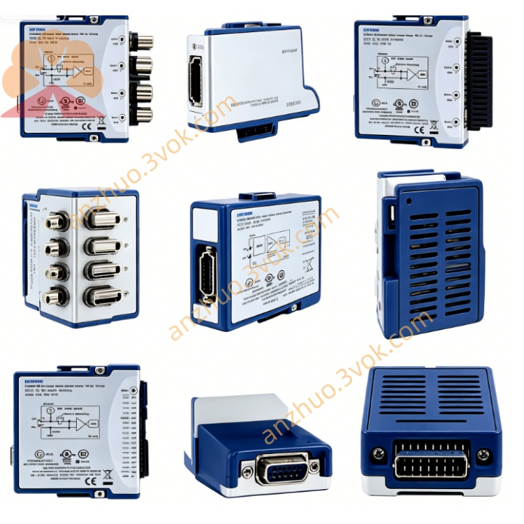
NI PXI‑5671 2.7‑GHz PXI RF Vector Signal Generator
Description
II. Model Interpretation
PXI represents that the equipment follows the PXI industrial bus specification and adopts a 3U external structure, occupying three adjacent chassis slots, and is compatible with both PXI and PXIe chassis.
5671 belongs to the NI RF Vector Signal Generator series, representing a medium-high frequency model with a maximum working frequency of 3.3 GHz and a real-time bandwidth of 22 MHz.
The product is differentiated by its onboard memory capacity. The component number for the 8-MB memory version is 778287-01, for the 32-MB memory version it is 778287-02, and for the 256-MB memory version it is 778287-03.
III. Technical Parameters
The following parameters are typical values after the equipment has preheated for 30 minutes under a 25-degree Celsius environment and a 50-ohm standard load.
1. Frequency and Timing Parameters
Operating frequency range: 250 kHz to 3.3 GHz
Real-time signal bandwidth: 22 MHz
Reference clock: 10 MHz constant temperature crystal oscillator
Frequency stability: ±20 ppb
Frequency accuracy: ±50 ppb
Phase noise: Less than -124 dB/Hz at 1 GHz carrier and 10 kHz frequency offset under the condition of -145 dBm to +13 dBm output power
2. Output Power and Signal Indicators
Output power range: -145 dBm to +13 dBm
Power resolution: 0.1 dB
Output attenuation: 0 to 90 dB, with a 10 dB step
Harmonic suppression: Greater than 60 dB carrier
Output impedance: 50 ohms
3. Sampling and Storage Parameters
Sampling bit number: 16 bits
Base sampling rate: 100 MHz samples per second, equivalent to 400 MHz samples per second after quadrupling interpolation
Onboard memory: Optional 8 MB, 32 MB, or 256 MB
4. Modulation Types
Supports amplitude modulation, frequency modulation, phase modulation, amplitude shift keying, frequency shift keying, phase shift keying, minimum frequency shift keying, orthogonal amplitude modulation, and other mainstream modulation formats
5. Physical and Environmental Parameters
Equipment specification: 3U structure, occupying three chassis slots
Overall power consumption: Approximately 36 watts
Operating temperature range: 0 degrees Celsius to 55 degrees Celsius
Cooling method: Forced air cooling of the chassis
IV. Interface and Communication Configuration
Front panel interface
RF output interface: Uses SMA interface, with an impedance of 50 ohms, for outputting RF signals externally
External reference clock input interface: Uses SMA interface, connecting a 10 MHz external clock to achieve multi-device synchronization
Programmable function interface: Used for connecting external trigger signals to complete timing synchronization between devices
Status indicator lights: Indicate the power supply status of the equipment and the clock lock status
Bus and software configuration
The device backplane integrates a standard PXI bus, including a 32-bit PCI bus, a PXI trigger bus, and a 10 MHz reference bus, enabling trigger linkage and clock sharing between devices.
The accompanying driver program is NI-RFSG, which can be used normally in common development environments such as LabVIEW, TestStand, Python, and C#.
With a dedicated modulation tool software, wave form editing, signal generation, and parameter analysis can be completed.
V. Core Functions
1. Covers the frequency band from 250 kHz to 3.3 GHz, with a 22 MHz bandwidth capable of meeting the simulation requirements of various medium-high frequency wireless signals, providing a wider range of applicable scenarios.
2. Built-in high-stability constant temperature crystal oscillator with high frequency accuracy and good phase noise performance, ensuring the purity of the output RF signal.
3. Adopting a 16-bit high-resolution sampling design, supporting multiple modulation methods, and allowing the loading of custom arbitrary waveforms to generate complex RF signals. 4. The power adjustment range is wide, with high adjustment accuracy. It can simulate weak signals and conventional power signals, meeting the various testing requirements of the receiver.
5. The modular design enables it to be used in conjunction with RF analyzers such as PXI-5660 and PXI-5661, forming a complete RF transmission and reception testing system.
6. It supports multi-device synchronous operation, sharing the same reference clock and trigger signal to ensure the phase consistency of multiple output signals.
Six. Application Scenarios
1. Wireless communication testing, used for the calibration of transmitters of second, third, and fourth generation mobile communication devices, Bluetooth, wireless local area networks, and radio frequency identification products, as well as the sensitivity and modulation accuracy detection of receivers. Suitable for medium and high frequency communication equipment.
2. RF component testing, conducting gain, loss, linearity, harmonic, and spurious index tests on RF amplifiers, filters, mixers, RF switches, etc.
3. Radar and electronic equipment testing, simulating medium and high frequency radar signals and various RF environments, completing equipment functionality and anti-interference performance tests.
4. Aerospace and defense field, used for the calibration of military RF equipment, RF link simulation, and RF sensor signal excitation.
5. Automotive electronics testing, conducting functional tests and anti-interference tests on automotive RF products such as remote control keys, tire pressure monitoring modules, car Bluetooth, and automotive RF radar.
Seven. Installation and Maintenance Instructions
Installation and Power On
The equipment must be installed in a power-off state, fixed to three adjacent slots of the chassis, and ensure reliable grounding of the chassis to prevent hardware damage from static electricity.
After installation, connect the power supply, and preheat continuously for thirty minutes to allow the internal constant temperature crystal oscillator to reach a stable working state. Use the NI MAX software to complete the overall machine self-check to confirm no hardware faults and normal clock locking.
During operation, ensure that the air duct of the chassis is unobstructed, and the working environment temperature does not exceed 55 degrees Celsius. Do not block the chassis cooling fan.
Cable Connection and Operation
The RF output port is connected using a 50-ohm standard SMA coaxial cable, tighten the interface to reduce signal reflection and transmission loss.
When working in synchronous mode with multiple devices, connect to an external reference clock of 10 MHz and enable the synchronization function.
Before downloading custom waveforms, confirm the onboard memory capacity of the device to avoid waveform truncation and signal distortion issues.
Daily Maintenance and Calibration
It is recommended to conduct a professional trace calibration once a year to compensate for parameter offsets caused by long-term use of the equipment. Daily use can utilize the built-in self-calibration function of the device to correct performance drift caused by temperature changes.
Regularly use a drying tool to clean the dust on the SMA interface surface to keep the interface dry and clean. When the equipment is idle for a long time, install dust caps on all interfaces.
The storage environment and usage conditions of the equipment should be free of condensation, with the humidity controlled between 10% and 90%. Keep away from strong electromagnetic interference equipment and vibration sources.
Do not plug or unplug the signal cables while the equipment is powered on to avoid the equipment being impacted and subjected to severe vibrations. Do not operate the equipment for a long time in an environment exceeding the rated temperature.
Get a Quote