
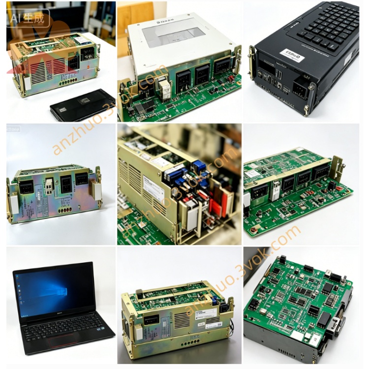
JANCD-GIO01
Description
Board interface and pins (key points)
1) Connector distribution (facing the component side)
CN1 to CN4: Input connectors (each 16 pins, total 64 inputs)
CN5 to CN8: Output connectors (each 16 pins, total 64 outputs)
CN9: 24V power supply and common terminal (COM)
LED: PWR (5V), RUN, ERR, I/O flashing
2) Power supply pin CN9 (must be connected)
1: +24V (external power supply positive)
2: 0V (external power supply negative / ground)
3 to 6: COM1 to COM4 (input common terminal)
7 to 10: COM5 to COM8 (output common terminal)
3) Input wiring (NPN/PNP universal)
NPN: Sensor output terminal → IN, COM connected to +24V
PNP: Sensor output terminal → IN, COM connected to 0V
Each point is connected with 1kΩ current-limiting resistor (already included in the board)
4) Output wiring
Transistor output: OUT → load → COM
Load: DC24V, ≤ 0.5A / point
Inductive load (relay / solenoid valve): Reverse current diode (1A/50V)
System connection and address
Slot: I/O slot next to the CPU board (GCP02/GCP03)
Bus: Backplane gold fingers (no additional wiring required)
Address: Default X0 to X77 (input), Y0 to Y77 (output) (octal)
With other boards: **GCP (CPU), GFG/GFL (communication), GIF (extended I/F)** in coordination
Common faults and troubleshooting
No response of the entire board (PWR does not light up)
Backplane 5V power supply abnormality, gold finger oxidation, slot damage
No signal input
External 24V not supplied, COM connected in reverse, optocoupler breakdown, terminal loosening
Output does not actuate
Output transistor damaged, COM not connected, load short circuit, program not set
Signal jitter / interference
Poor grounding, large 24V power supply ripple, and laying in the same slot as power lines
Get a Quote